This thread has been locked.

If you have a related question, please click the "Ask a related question" button in the top right corner. The newly created question will be automatically linked to this question.

Connecting J1708 to SN65ALS180 and SN65LBC184

Other Parts Discussed in Thread: SN65ALS180, SN65LBC184, DS36277, SN65LBC180

Is it possible to connect J1708 signals to the SN65ALS180? If so what are some of the recommended configurations and best practices?

What I would like to do is establish a J1708 data bus that has three nodes. Two of the nodes will be utilizing the SN65LBC184 driver configured according to the best practice methods and recomendations in data sheets. However, the third node will be connected to this J1708 bus using the SN65ALS180. I need to find out if this is possible and if so, how to configure the SN65ALS180 appropriatley.


Thank you.   

  • 1) While I will draw the circuit for you may I ask why you intend to use the SN65ALS180 device? It is a full duplex, high speed transceiver with switching time of 8ns. The J1708 bus uses approximately 10kbos only. You could generate a lot of noise with the fast transient times of the SN65ALS180.

    2) We also have the DS36277 to offer which already includes the inverter in the Driver Enable path. So you could reduce your logistics by utizing thre times the same device. Of course the DS36277 lacks the internal transient supressors of the SN65LBC184.

    The above are suggestions only just in case you were not aware of the avialble solutions.

    regards, Thomas

  • Please find attached the schematics for your SAE J1708 bus circuitry.

    regards, Thomas

    J1708.pdf
  • Thank you for the explanation and the drawing. I truly appreciate your help with this.

    The reason I intend to use The SN65LBC180, is because this is not a new design and that's all I have to work with.

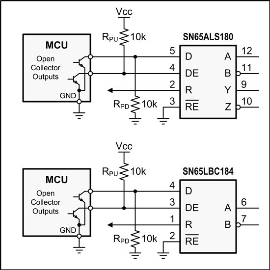
    I have the exact same set up as depicted in your drawings except for one thing. There is no inverter on the DE pin. Instead it uses a pull up resistor configuration as shown in the attached images. Please let me know what you think of this configuration.

    Thanks again.  

    0535.RS485__J1708_config.docx


  • It looks like your DE inputs are driven by an open-collector or open-drain output. In this case the open-collector output already provides the inverted version of the transmit input signal at the transistor base.

    What surprises me is that the D lines are not grounded. They seem to go to similar output stages as the DE lines. In this case I recommend to connect  pull-down resistors from the D lines to ground to ensure low-potential during power-up.

  • Yes, the DE inputs are driven low by the MCU. I will definitly take your recomendations in to consideration if I am able to redesign this part of the logic board. Right now, I am sort of stuck with the current board design that is already in use.


    Thanks again for all of your replies and assistance with this. You've been a great help and have taught me a lot.