This thread has been locked.

If you have a related question, please click the "Ask a related question" button in the top right corner. The newly created question will be automatically linked to this question.

ISO5500 de-saturation function

Other Parts Discussed in Thread: ISO5500EVM

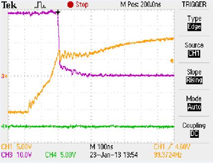
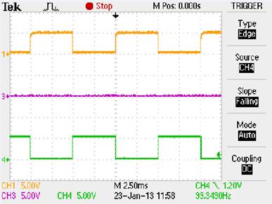
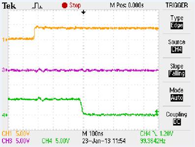
I am currently evaluating the Texas Instruments ISO5500 igbt driver and I am not able to use this part with the de-saturation function activated.  I am using this device with the evaluation board made by Texas Instruments.

Any suggestions?

  • Hi Shahzad,

      How do you have the ISO5500EVM configured and how are you trying to use the DESAT function?   Is JMP2 installed, and if so, it disables the DESAT function (see 2.1.2.2 in the User Guide).

      And when you say you are not able to use it, what are you seeing and what are the symptoms?  Waveforms/'scope capture such as in Fig 59 in the datasheet would be very helpful.

    -Leonard


  • I am using the evaluation board to power/control an igbt which is mounted on a heatsink.  I have short wires (5 in.) connecting the igbt to the evaluation board.  The reset pin is jumpered to gnd1.  The igbt is connected as a low-side drive. 

    When I have JMP2 installed I am able to pwm my igbt successfully.  IGBT is switching a heater load of about 8 amps.  The supply to the load is 37 VDC.  The graph below shows CH1= tp6 signal (gate drive) and CH3= tp7 signal (igbt collector). 

    When I remove jumper JMP2  tp6 goes to -10 VDC and stays there so the igbt is off all of the time.  If I look at what is happening on the input side of the ISO5500 I see the following: CH1= tp4= Vin 100hz 50% duty cycle control signal, CH3=tp2= reset input (always low), and CH4= tp1= fault output.  The below information tells me that the driver is sensing a desaturation fault every time that it tries to close the igbt c-e.  The interesting thing is that if I monitor the driver output I am not able to see it go high at the beginning of every cycle.  This makes no sense.


     In addition, I would like to know if I can connect gnd1 and Vee together in order to be able to monitor all of the driver inputs and outputs without damaging the driver.

     I wonder if the driver’s internal current driving capability is not powerful enough to drive the igbt without external drive transistors.  In our target production design we are planning on using these external transistors but with my quick test prototype I am not using the transistors.

  • Shahzad, your assumption is most likely correct. If the drive capability of the ISO5500 is not sufficient for your IGBT, the transistor won't turn on fully and thus causing a DESAT voltage above the DESAT threshold. Can you measure the voltage at the DESAT pin to confirm this?

    Also you mentioned you are using a 37V supply. However the ISO5500 is only specified to 35V maximum. The recommended range is actually 5V below that!, so 30V.

    I'm still surprised that the /FAULT pin toggles though since you have jumpered the /REST-pin to Ground. The /RESET pin controles an internal RS-latch so /FAULT should stay high all the time. I will see the chip designer tomorrow and discuss this situation with him.

    Regards, Thomas

  • The 37VDC is the power to the load not to the driver.  I am using +15V and -10V, so 25VDC for the output power supply on the driver.  5V to power the input side of the driver.

     As mentioned earlier, I do not see a signal on the driver output and because of this I will not be able to see a desat input to the driver since the igbt is not being toggled without an input when I remove the JMP2 in order to operate the driver with the desat function.

     I do notice from the graph below, same as the previous one I sent you but exploded, that after Vin goes high a faut signal is sent by the driver only 330 ns after the Vin high signal.  The data sheets of the driver state that the desat blanking time = 2.7 µs with the Cblk provided on the evaluation board.  Therefore, it makes no sense that we are receiving a fault signal sooner than the blanking time.  (CH1= Vin+, CH3=reset input, CH4= fault output.)

    My new theory is that it is possible for the driver to be detecting a desat fault but after it detects the fault it goes into a mode not described in the data sheets, a mode which produces what I am seeing and caused by the fact that the reset pin is always in the low state.  From what I can see the reset signal should be sent only after the Vin+ signal goes low.

     Could we possibly arrange a con-call as my customer's window is closing in and he needs to get this figured out very quickly?

  • My theory is that something with the evaluation module might be wrong. Unfortunately I have not designed this board and I am new to this board. Therefore I will have to order one to measure it for myself. In the meanstime could please check your board and see whether D1 is installed and that D2 is replaced by a wire bridge. It is possible that our assembly house might have done exactly the opposite and replaced D1 with a wire bridge and inserted D2.

    One I receive the board I will copy your set-up and investigate.

    regards, Thomas  

  • We checked out the EVM and everything works fine. When connecting DESAT to Vcc2 we could confirm your scope shots. We therefore suspect your DESAT-pin somehow receives a voltage that is higher than the DESAT threshold from somewhere. This might be due to a short or a wrong connection due to solder work. This was also the reason why I asked you to measure the voltage at DESAT with regards to VE.

    There is nothing wrong with the Chip or the EVM. Please check you DESAT voltage.

    Thank you and best regards,

    Thomas