This thread has been locked.

If you have a related question, please click the "Ask a related question" button in the top right corner. The newly created question will be automatically linked to this question.

DS25MB100 recommended page 14 land pattern doesnot give any information about the DAP or center pad also dimesions for the same

Other Parts Discussed in Thread: DS25MB100

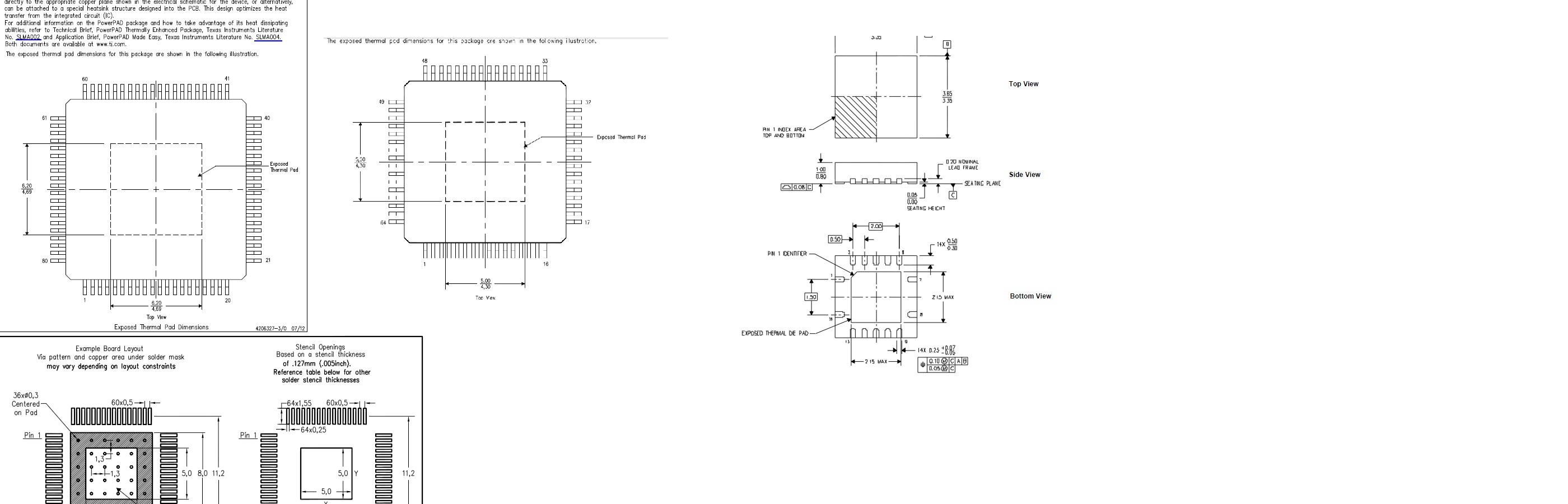
 Please advise if some one looks at this created the library then it sill problem  also not provede the dimensions of DAP or GND PAD.

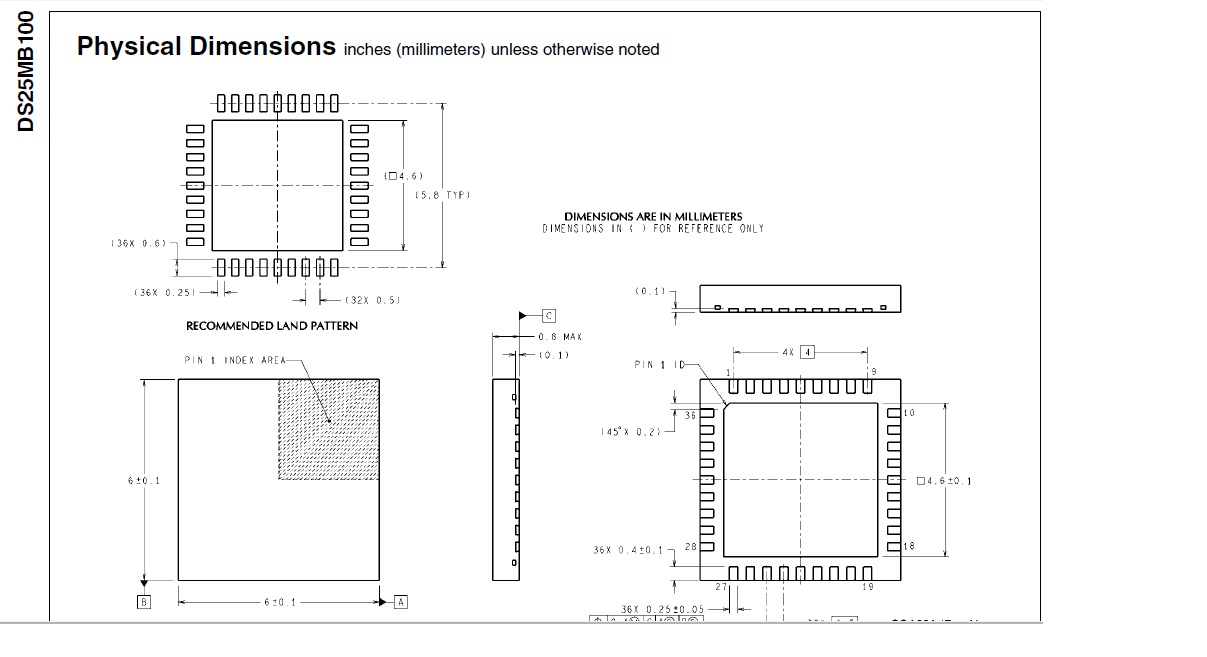
do you think is this the time to change the land patteren to match with Order Number DS25MB100TSQ which is shown in page 3

Kindly advise

  • please find other datasheets of TI where recommended land pattern shown. so DS25MB100 page 14 does not shows the thermal pad anywhere as well as dimensions for the same. kindly do the modifications if its wrong so that  if some one looks at this created the library then it sill problem  also not provide the dimensions of DAP or GND PAD.or thermal pad.

    do you think is this the time to change the land pattern to match with Order Number DS25MB100TSQ which is shown in page 3

    Kindly advise

  • Sathya

    I will look into the package drawing in the datasheet, but in the meantime, I'd like to suggest that you look at this application note: http://www.ti.com/lit/an/snoa401q/snoa401q.pdf

    AN-1187 provides a lot of information on the package used by the DS25MB100.

    Mark

  • The DS25MB100 datasheet on the web shows the correct package drawing.  The dimensions for the DAP are shown (4.6 mm square) as well as the recommended land pattern to use for the PCB.

    Gary Melchior

  • Thanks Gary for the information on the dimension of DAP i will use the same but clarification required is in the recmonded land pattern They never mentioned  its exposed thermal pad or DAP or center pad they would have mention to clear the   expected doubts arise on the same . they no where mentioned the stiching pads attach to center pad so iwould like to know is it good to mention in the land patteren recmondation sheet to avoid problems.

  • this is what i was talking about after going through application note like in this data nowhere mention anywhere DAP length also no where mentioned as Center pad or thermal pad or DAP like i attached few from ti data sheets also sent by you.

  • The package DAP dimension is shown on the package drawing (off on the right side), as 4.6mm,  Recommended Land Pattern, also on the datasheet, also shows the suggested center pad which is also 4.6mm square.    I am not sure I understand what it was that you were not able to find.

  • yes they never mention its center pad ir thermal exposed pad or atleast DAP in this recmonded land patteren page as i attached in my second message  like other data sheets. thanks still not convienced sorry please check my 2nd message attaching recmonded land patterens from different datasheets from Ti  thanks

  • since datasheets should have accurate but in this case assumptions are made that its center pad or DAP which is not mentioned anywhere in fhis page kinsly eecheck if you find anything like in other datasheets from Ti DAP width &DAP height or center pad showing as DAP dimension or thermal exposed pad  that is where i am suggesting to change to maintain conaistency between data sheets  kinsly advise  if PCB designer looked at this page while creating library its really  hard to get since