This thread has been locked.

If you have a related question, please click the "Ask a related question" button in the top right corner. The newly created question will be automatically linked to this question.

Where is the TUSB2136-TPS2149 Product Development Kit Sample Source Code?

Other Parts Discussed in Thread: TPS2149

The TUSB2136-TPS2149 Product Development Kit Getting Started says: "The Sample Source Code can be downloaded if you agree to the online royalty-free license agreement. Objext code comes pre-loaded in the on-board EEPROM."

Where can I download the sample source code that is referred to?

When I plug in the TUSB2136-TPS2149 Product Development Kit into the USB, the power light comes on, but the Windows Device manager says the device is unknown and the driver is not loaded.

What Windows drver is needed for this device and where can I get up?

Please help to get this TUSB2136-TPS2149 Product Development Kit up and running on Windows.

  • Hello,
    Driver, schematics and User's Guide are available at the Device's web page under the "software" and "application notes" sections.

    Here http://www.ti.com/tool/tusb2136tps2149pdk or here http://www.ti.com/product/TUSB2136/toolssoftware

    Regards
  • Sample software is not located at http://www.ti.com/tool/tusb2136tps2149pdk or http://www.ti.com/product/TUSB2136/toolssoftware.

    Where is the sample software located and where is the Windows driver software for the keyboard application?
  • Hi Don,

    Please send me an e-mail to JoseCarlos.Gil@Ti.com I can send to you the keyboard software.

    Regards.
    JC
  • I still do not have the Sample software or know where to get it.
  • I have sent by mail.
    Regards.
    JC
  • I have not received email with schematic or sample code as yet that should have been supplied with the Kit.


    Where cn I get this information?


  • Hi Don,

    As I have mentioned you by mail, you can go to this link:
    http://www.ti.com/tool/tusb2136tps2149pdk?keyMatch=tps2149&tisearch=Search-EN
    and scroll down to reach the "Design Files", "User Guides", "Application Notes", "Software" etc.
    Under "Design Files" you can find the main EVM Schematic and Keyboard Schematic which belongs to the boards with the two headers of 7x2 like yours.

    Let me know if you need more help.

    Regards
    JC
  • This schematic http://www.ti.com/lit/df/sllr043/sllr043.pdf has the 9x2 headers.
    This schematic http://www.ti.com/lit/df/sllr042/sllr042.pdf has 7x2 headers but doesn't tell me where the test points are located on the board.
    There are many more test points on the board then are located on the http://www.ti.com/lit/df/sllr042/sllr042.pdf schematic.

    Where are the test points, that are indicated on the schematic, located on the board?
    What do the other test points, that are not indicated on the schematic, do and where are they located on the board?
    THANKS.
  • Hi Don,

    TUSB2136_EVM_pcb.pdf

    I'm attaching the PCB layout where you can see where are the test points located, those are marked, also, you can see in the schematics hat those test points are indicated with a "Y"

    Please let me know if you need more help.

    Regards
    JC

  • The PCB has more than 7 test points on it.
    I need to know what each test point is located on the PCB and what each one does.

    All test point on the PCB should be labeled on the PCB with the same lables that appear on the schematic.

    I need this information to be able to use the Kit.

    Please provide this information.
  • Hi Don,

    The pictures I have attached was just an example on how to locate the test points and in fact, the test points in the PCB are labeled just like in the schematic (no labels on either).
    Did you open the files to see the whole picture?
    I think it would be better if you tell me what test point are you looking for so I can tell you exactly where is it or you can tell me what exactly do you want to test and I tell you how to do it.

    Regards.
    JC
  • I do not have an answer yet to my questions.

    1. The board is supposed to be programmed with a keyboard application.
    When I plug the board into the PC USB, the D1 LED lights saying the board is good.
    The Windows Device Manget shows that a new USB Hub device was plugged in, not a keyboard.
    If I run Notepad and press a keyswitch on the PCB, no text is entered into Notepad. It should.
    If I plug a USB keyboard into a downstream USB connector on the PCb, Device Manager does not show the keyboard present. It should.
    Obviously neither the Keyboard nor the USB Hub application are working correctly on the PCB.
    How do I get the application on the PCb to wor correctly?
    I need the source code of the application to be able to fix this.

    2. The are about 2 dozen test points on the PCB, all of them unlabeled.
    The PCB schematic also does not have the test point labeled.
    How can I find out what each test point does and where it is located on the PCB?
    How can I debug my evaluation of the Kit without using the test points?
    Please provide documentation on all of the test points and where they are located on the PCB.

    This issue is not resolved until:
    1. I get an accurate schematic of both PCBs in the kit.
    2. The application on the PCb functions as it is supposed to.
    3. I get source code of the application so that I can debug it.
    4. I get documentation on all of the test points, what they do and where the are located on the PCBs.

    I need to be able to do a proper eavl of this kit, the TUSB2136 chip and my modifications of the kit(yet to be done).
    I need technical suppor to be able to do this and to put a TUSB2316 design into production.
    Please help.
  • Don,

    As I have told you before, all the information you're asking for is on the next link:

    http://www.ti.com/tool/tusb2136tps2149pdk?keyMatch=tps2149&tisearch=Search-EN

    All you have to do is to scroll down to find "TECHNICAL DOCUMENTS" in that section you can find "DATASHEETS", "APPLICATION NOTES", "USER GUIDES", "DESIGN FILES"and "SOFTWARE"

    EVERYTHING is there.

    1. I have sent accurate schematic of both PCBs in the kit.
    2. You will get the application on the PCB function as it is supposed to do once you have download and read the user guides
    3. We don't share the source code of any device, what you can get is the software needed to run the device and you can dounload from the link I have mentioned.
    4. I have sent diagrams to show where is each test point indicated in schematic and also in PCB, and the function of each est point becomes obvious when you see the schematic, but you can refer to section 3.5 of the EVM user's guide.

    Regards.
    JC

  • 1. Rurrenly, I do not have an accurate schematic that also includes all of the test points that are on the PCB.
    2. Downloading and Reading the User guides, which I have done does not get the application to perform as either a Keyboard or a USB Hub, as it should.
    3. Without the source code I will not be able to get the board to perform the application properly.
    4. I do not have any documentation, including the disgram that you sent, that telles me what each of the two dozen test point on the PCB do and where they are located. Without this I will have trouble usin the kit to perform my evaluation.

    It is too bad that I cannot get the information from you that I need to evaluate the TUSB2136 chip for my application.

    I still need the information that I requestedabove.

    Answer me this question: How many test points are on the PCB and do you know the function of each test point? Neither do I.
    Please provide this information.
  • Don,

    I have sent before the file named TUSB1236_EVM_pcb.pdf in which you can see below image:

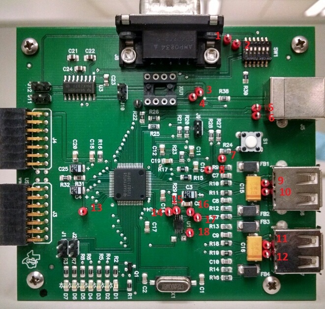
    It has 18 test points and in the schematic found in this link:  you can see what for each test point is. 
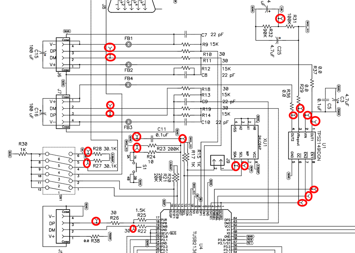
    If you pass this files to the electronics engineer on charge of the project he will understand with no doubt the function of every test point, for example, the test points on SCL & SDA are to test communication with the EEPROM, the test points on DP & DM lines are to test usb communication and so on, just give this files to the electronic engineer on charge and there should be no misunderstanding.

    Regards.
    JC 

  • Hello  Don,

    Here you go the reference for all the 18 test points on the board, please notice that all you need to understand each test point, is to analyze the schematic and the PCB layout.

    1.- S3 pin of the TUSB2136

    2.- S2 pin of the TUSB2136

    3.- SDA pin of the TUSB2136

    4.- SCL pin of the TUSB2136

    5.- Upstream DM pin of the TUSB2136 (DM0)

    6.- Upstream DP pin of the TUSB2136 (DP0)

    7.- RST pin of the TUSB2136

    8.- DVCC 3.3V

    9.- DP1 pin of the TUSB2136

    10.- DM1 pin of the TUSB2136

    11.- DP2 pin of the TUSB2136

    12.- DM2 pin of the TUSB2136

    13.- 1.8V

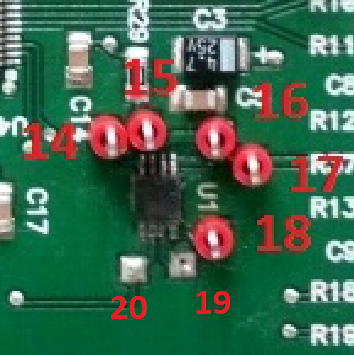
    14.- Out2 pin of the TPS2149IDGN, Downstream VBUS2

    15.- VregOut pin of the TPS2149IDGN, DVCC 3.3V

    16.- VIN pin of the TPS2149IDGN, Upstream VBUS (5V, POWER signal)

    17.- Out1 pin of the TPS2149IDGN, Downstream VBUS1

    18.- EN1 pin of the TPS2149IDGN, PWR01 pin of the TUSB2136

    Best regards,

    Diego.

  • Hello Don,
    Regarding the points 1 2 and 3.

    1) Yes you have the accurate schematic, it includes all the 18 test points on the PCB (I know it because I used one of the references that you previously posted, in order to enumerate and describe each test point)

    2)Could you verify if the EVM has an EEPROM with a valid firmware. If it has an EEPROM, then you can update the firmware by following the firmware programming flow user's guide http://www.ti.com/lit/ug/sllu020a/sllu020a.pdf

    3) Texas Instruments does not provide source codes, the software development is under the customer's responsibility.

    Regards,

    Diego.

  • My PDK PCB has 20 test points on it, not 18.

    That means that your schematic is inaccurate and does not reflect the actual PCB that I have..

    Surely, you have accurate schematics and documentation on the PDK boards that you are shipping to customers.

    Please send me an accurate schematic of the PCB that you shipped to me with the function and location of each of the 20 test points that are on the PCB.

    THANKS for your assistance.

  • Can you upload a picture of the board you have?

    Let me know if you need assistance in uploading a picture.

    JC
  • Hello Don,

    The board has two unpopulated testpoints, which should be located around the TPS2149. Please see the picture below to locate the points on the board.

    19.- EN2 signal of the TPS2149, PWR02 signal of the TUSB2136

    20.- OC signal of the TPS2149, OVCR1 & OVCR2 signals of the TUSB2136

    Again, the schematic you have is correct, because the missing test points on my board still match with the schematic you have. Indeed the schematic has an extra test point which is not being populated at all doe to its connected to DVCC_33 (3.3 V). Here is a screen capture which contains a red circle on all the test points:

    Regards,

    Diego.