This thread has been locked.

If you have a related question, please click the "Ask a related question" button in the top right corner. The newly created question will be automatically linked to this question.

wrong pulse about SN65HVD24

Other Parts Discussed in Thread: SN65HVD24

Hi,

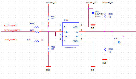
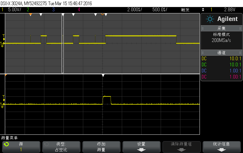
when I use SN65HVD24 to act as a receiver,it has a pulse on R pin about 0.8us before the valid data. The next scope is 2400bps.when I use 9600bps, all valid data become zero level.Is the circuIt's schematics right?What is the problem?

Thanks a lot.

  • Hello Zehua

    Firstly, As you see in table "Receiver Equalization Characteristics" (in datasheet) this device can work at 5 Mbps with 500 m and 1 Mbps with 1000 m.

    On the other hand, if you want to receive data, I recommend you to take out the pull-up and pull-down resistors in the input and just use the R162, also take out R160 and R163.

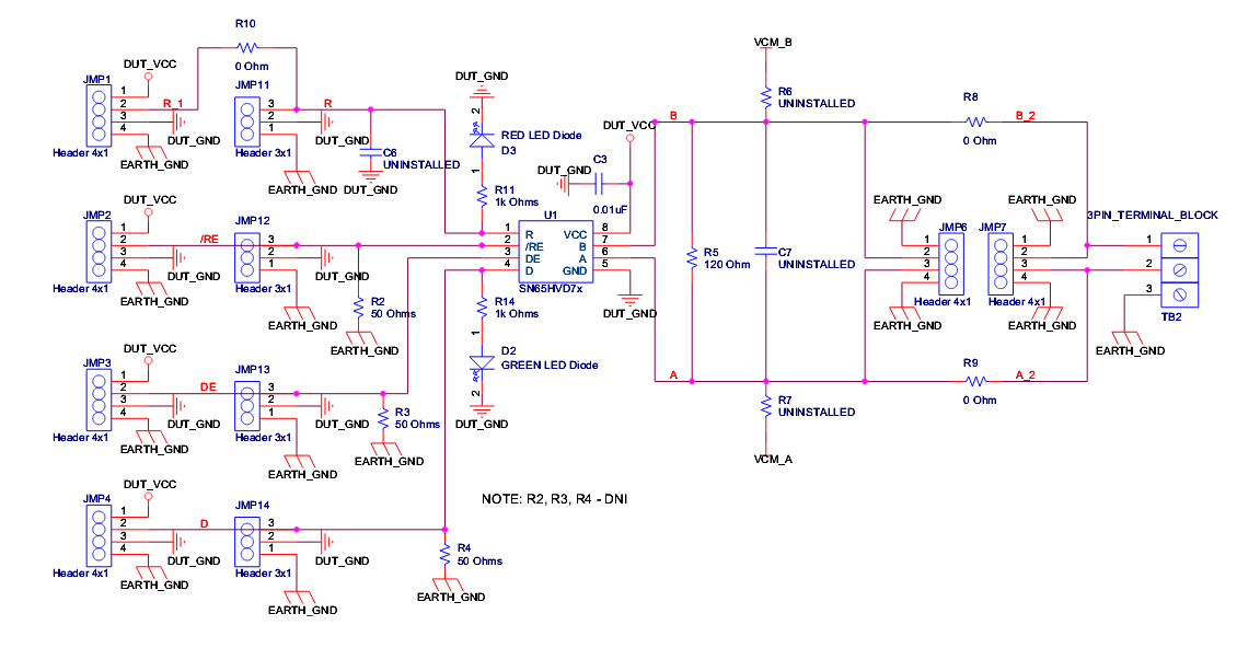
    I let you a diagram of the EVM configuration.

    If you can, please send me more information about your application, could be better.

    Please check it out and let me know your comments.

    Regards

    Francisco

  • Hi Zehua,

    I'm also curious: does this pulse happen only after the /RE pin toggles from high to low, or does it occur when /RE is static low but before data is received on the bus (A and B) inputs?

    Regards,
    Max
  • Hi Francisco,

    Thanks for your support.

    I control DR&RE pin to switch between Receiver and Transmitter.

    I did as you said and it works.But there is still one pulse after the Stop-bit. Why?


  • Hi Max,

    It occurs when /RE is static low.After I disconnect the four resitance,the pulse before Stop-bit disappears, but one pulse after Stop-bit occurs instead.

    It is very strange,do you have some suggestion?

    Thanks!

  • Hi Zehua

    Can you send an screen-shot of the A, B and R signal? If possible, please put DE_/RE signal as well. Do this test without R4, R3 and R2.

    Please, let me know your comments.

    Best Regards
    Francisco
  • Hi Francisco,

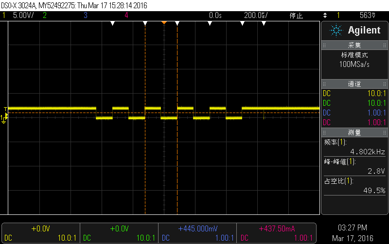
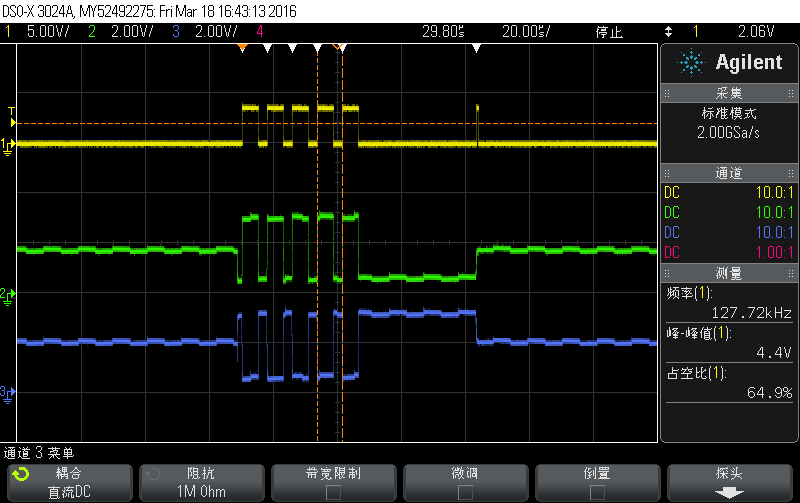
    FYI, scope 1 is R signal, scope 2&3 is A,B signal. All of pull-up and pull-down resistances  of input and output  are removed.

     ,

  • Hi Zehua,

    When the driver is disabled, it looks like there is a negative offset on the differential signal that is causing the voltage at B to be higher than the voltage at A (so that the bus is at a logic low state during idle periods). Do you know why this is? If your pull-up/pull-down resistors (R161 and R164) were populated then there should be an offset in the positive direction, and if no resistors were populated except for the termination (R162) then the signal should have almost no offset (meaning voltage at A = voltage at B).

    I think this negative offset during the idle periods is what is causing the glitch. Before the driver is disabled, it is sending a low level. As the driver shuts off, the A and B waveforms will approach each other. For a short time they may be close enough that the high-level input threshold of the receiver is exceeded. (This device actually has a high-level threshold that is a low negative number. This is so the R output is a high level when the differential input is 0 V. This is useful since it gives a known output in conditions where the bus is idle or shorted.)

    Regards,
    Max