This thread has been locked.

If you have a related question, please click the "Ask a related question" button in the top right corner. The newly created question will be automatically linked to this question.

DS26LS31C: High voltage driver 12 or 24VDC

Part Number: DS26LS31C
Other Parts Discussed in Thread: SN74LVC1G57

I am using DS26LS31C for driving high speed optocoupler which is on different  board. Max cable length is 10ft and I have used twisted pair shielded cable. Max transfer rate required 1Mbit/sec. Environment is very noisy and hence looking for driver IC which has 3.3/5 volt input and differential output with 12/24 Volt DC signal.

Pl suggest suitable alternative which can handle 12 or 24 Volt DC  differential signal.

  • Hi Mahesh,

    It is rare to find differential drivers with such large differential output voltages, since the use of balanced signaling in general is typically sufficient to overcome environmental noise (which couples onto the common-mode component of the signaling and is thus rejected by the differential receiver).

    Have you encountered issues with your current set-up due to noise? Are you driving the optocoupler directly from the differential line, or do you have a receiver circuit to convert the differential signaling into single-ended logic-level (3.3 V or 5 V) signals first? If you could show a schematic or block diagram it might help us better understand the problem you are trying to solve.

    Regards,
    Max
  • Hi Max,

    Thanks for your immediate reply. Find below schematic.

    Signals are traveling from PCB1 to PCB2 and environment is very noisy. ( Higher noise due to nearby DC pulsating current-200amp peak and DC spark) 

    Regards,

    Mahesh

  • Are you currently using the second channel of the optocoupler? If not, there are methods to use the second channel to improve the common-mode rejection by a large amount.
  • Mahesh,

    Clemens's suggestion sounds worthwhile to me, too. Another approach would be to use an RS-485 or RS-422 receiver on PCB2 to receive the differential signals and convert them to a single-ended output (that would then drive HPCL2631). These receivers are typically designed to operate well in noisy environments by rejecting common-mode noise.

    Max
  • Currently I am using second channel of optocoupler. But I need to change design due to noise problem. Can you suggest method to improve noise immunity using second channel?
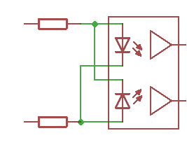
  • Use a differential driver (i.e., transmit current in different directions for 0 and 1 bits) and connect both LEDs with opposite polarity:

    (Using two symmetrical resistors slightly increases the noise resistance.)

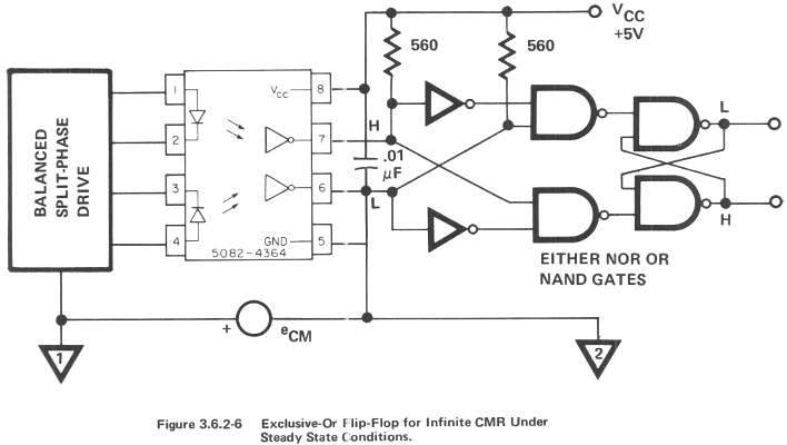
    Then use the two outputs to reconstruct the original signal (as shown in section 3.6.2 (Common Mode Rejection (CMR) Enhancement) of HP's Optoelectronics Application Manual):

    […]

    A selective flip-flop output circuit can take advantage of a situation in which the eCM transients have a higher rate of change in one direction than in the other, such as a sawtooth. It can also take advantage of a circuit with CMH > CML or vice versa (see Section 3.2.1). Since a NAND flip-flop can tolerate having both inputs high, it should be used where the likelihood is greater for both isolator outputs to be high (due to eCM transient) than is the likelihood that both outputs will be low. Conversely, a NOR flip-flop can tolerate having both inputs low, so the rule is reversed. These rules are summarized in Figure 3.6.2-5.

    Exclusive-OR flip-flop, whether of NOR or NAND construction can tolerate either both inputs high or both inputs low without either of its outputs changing state. The outputs can change state only in response to a change in differential input, so it has infinite common mode rejection for a static condition of eDM in either logic state. […]

    CAUTION: although the exclusive-OR flip-flop has infinite static immunity to eCM its dynamic immunity is not infinite. If a common mode transient capable of holding both isolator outputs either high or low should persist throughout the duration of a differential mode pulse, the pulse will escape detection. Other than this, the worst a common mode transient can do to the exclusive-OR flip-flop is to advance or retard the timing of the flip-flop output transition, i.e., cause jitter of the edge.

    With two NOR gates, you get an S/R latch. With two NAND gates, you get an S/R latch.

    To implement the "XOR flip-flop" in the bottom figure, you can use two SN74LVC1G57 devices to get two "NAND-with-one-inverted-input" gates, and a third SN74LVC1G57 to implement the S/R latch (actually, a JK latch) by feeding back its output to its third input.

    To further increase common-mode rejection, use higher currents. Section 3.6.1 shows various line termination schemes which you probably do not need.