Because of the Thanksgiving holiday in the U.S., TI E2E™ design support forum responses may be delayed from November 25 through December 2. Thank you for your patience.

This thread has been locked.

If you have a related question, please click the "Ask a related question" button in the top right corner. The newly created question will be automatically linked to this question.

TPS2066: Glitch on OC pin at TPS2066D power-up

Part Number: TPS2066

Hi,

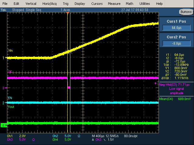
We are currently using the TPS2066D as load switch for USB ports. y at the VIN pin ramps up, a glitch occurs on the OC# pin while VIN is still very low (~ 0.72V). This glitch is sometimes interpreted as an overcurrent event by the USB controller and causes port malfunction. There is nothing else connected on the line between the switch and the controller, so this glitch must be issued by the TPS2066D itself.

I would like to know if this is an expected behavior for this component. I know there is an UVLO feature that should prevent malfunction while VIN supply is below a certain range, but in our case this feature does not seem to prevent the OC pin from glitching.

See attached scope capture.

Thank you.

Cedrick

  • Hey Cedrick,

    This is intriguing, could you send along a schematic of this block of your circuit? If you are concerned about IP issues let me know and we can work something out. In the meantime I'll dig around to see if I can find the cause.

    Best Regards,
    Nick
  • Hi Nick,

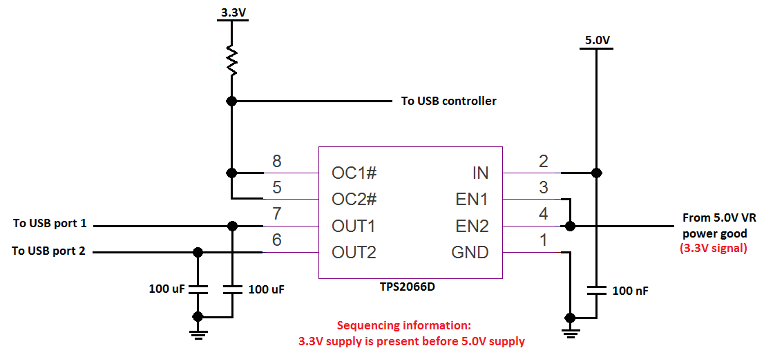
    Thanks for your fast reply. To work around potential IP issues, I have attached a sketch of the circuit. The circuit itself is pretty simple, so there should not be much information missing. Please let me know if this is not sufficient.

    I would like to point out also that the glitch occurs whether a device is connected to the USB port or not.

    Thanks for your help

    Cedrick

  • Hey Cedrick,

    I've looked into this and I'm pretty sure that your issue has something to do with power sequencing. It has no mention of it in the datasheet, supporting literature, or erratas but I bet that the inputs to the OR gate that drive the "deglitch" circuitry are being toggled at startup. The UVLO feature may be working correctly since it is intended to keep the outputs from going high which it seems to have do for you I think. I've ordered the chip to try and confirm that this is in fact the issue, it should be here tomorrow in the afternoon. In the mean time, would you be able to ramp tie the OC pins to the 5V supply so they ramp at the same time; let me know if you still see this glitch. If you don't, I think we've nailed down the culprit, is there a reason that you had connected it this way, did I miss a layout instruction in my reading?

    Here is the recommended circuit layout from the EVM Guide for this part which would seem to imply that these pins should be ramped together:

    Best Regards,

    Nick

  • Hi Nick,

    I have measured the OC pin behavior when pulled-up to the 5V supply and can still see the glitch when the 5V rail ramps up to around 0.8V (I'd bet this is the threshold where internal logic begins to work). However, I do not think this glitch would be an issue in such application because it occurs while the supply is still in the CMOS/TTL low level range.

    Our implementation though is part of a more complex system that requires the USB controller to stay active during low power states. This is why the OC pin needs to be maintained high at all times, independently of the input rail. The problem as you mentioned seems to be related to sequencing, i.e. the 5V supply turning off in low power states. It's sad there is no mention of the scope of the UVLO feature in the technical documentation because we assumed it would prevent such behavior on the OC pin and not just on the output pin.

    I will wait on your feedback from the tests you will run on your side to confirm you can see the glitch as well and this behavior is not related to a specific lot. We might have to modify the circuitry to either filter the glitch or change the power supply sequencing. Do you have any other suggestions?

    Best regards,

    Cedrick

  • Hey Cedrick,

    Parts got in yesterday afternoon, will go run a few tests on them later this morning to see if I can verify what you're seeing.

    Best,
    Nick
  • Hey Cedrick,

    Just got out of the lab, it appears that it is the logic kicking in at that time. In my runs I was able to get similar pulls of the OC line where the pull was varied from about 50ns to 80us depending on the resistance value. Unfortunately it looks like you're stuck with the "feature" of the device.

    A solution could be to implement a logic gate to replace the OC pins. The function I believe you'd need is Y = A' + B which in your terms would be newOE = VCC' + OC. This can be completed with a simple inverter and OR gate from TI which are incredibly small and quite inexpensive. Alternatively, if you use the SN74LVC1G57 you can get this same functionality in one device with six pins if you tie "in0" and "in2" together and then make that VCC; "in1" would be OC I believe. 

    A = VCC

    B = OC

    If this answered your question then please verfiy the solution below by hitting the green verification button; it helps to know that we could lend a hand and allows others to more easily find the solution to similar problems! If you have additional questions then just send them my way and I will work to answer them for you.

    Best Regards, 

    Nick