This thread has been locked.

If you have a related question, please click the "Ask a related question" button in the top right corner. The newly created question will be automatically linked to this question.

DS90LV001: IN+&IN- Pin Connection On The Schematic

Part Number: DS90LV001

Dear TI support team

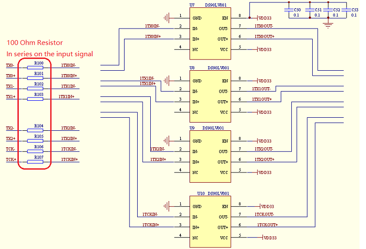
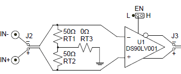
        We used 4pcs DS90LV001 to design the LVDS To TTL Schematic.When we did sample test with customer's system(not EVM),we found some of resistor in series on the input signal had small probability to be  broken down randomly,but DS90LV001 was fine.The value of Resistor is 100 Ohm beacuse it can prevent the LVDS dispaly abnormally.But we found  the different connection on DS90LV001 reference design that the IN+&IN- Pin connect a 50 Ohm Resistor to GND respectively.

Was my connection right? Is there a risk that inrush current happen to break down the series resistor? If my conection is OK,what is the appropriate value of the series resistor?

Customer‘s Schematic:


DS90LV001 Reference Design:  

  • Yulei,

    The DS90LV001 does not include TTL or LVCMOS outputs.  This device is just a LVDS buffer.  For LVDS input signals the recommended values for RT1 and RT2 are 50 ohms each.  The value for RT3 should be open.  Resistors RT1 and RT2 are usually combined into a single 100 Ohm resistor to save board space.

    The fact that you are blowing up the series 100 Ohm resistors is concerning.  This could be a problem with GND reference, or a charged cable.  Where do the TX[2:0] and TCK signals originate?

    Regards,

    Lee