Other Parts Discussed in Thread: LMH0387, LMH0384, LMH0303
Hi
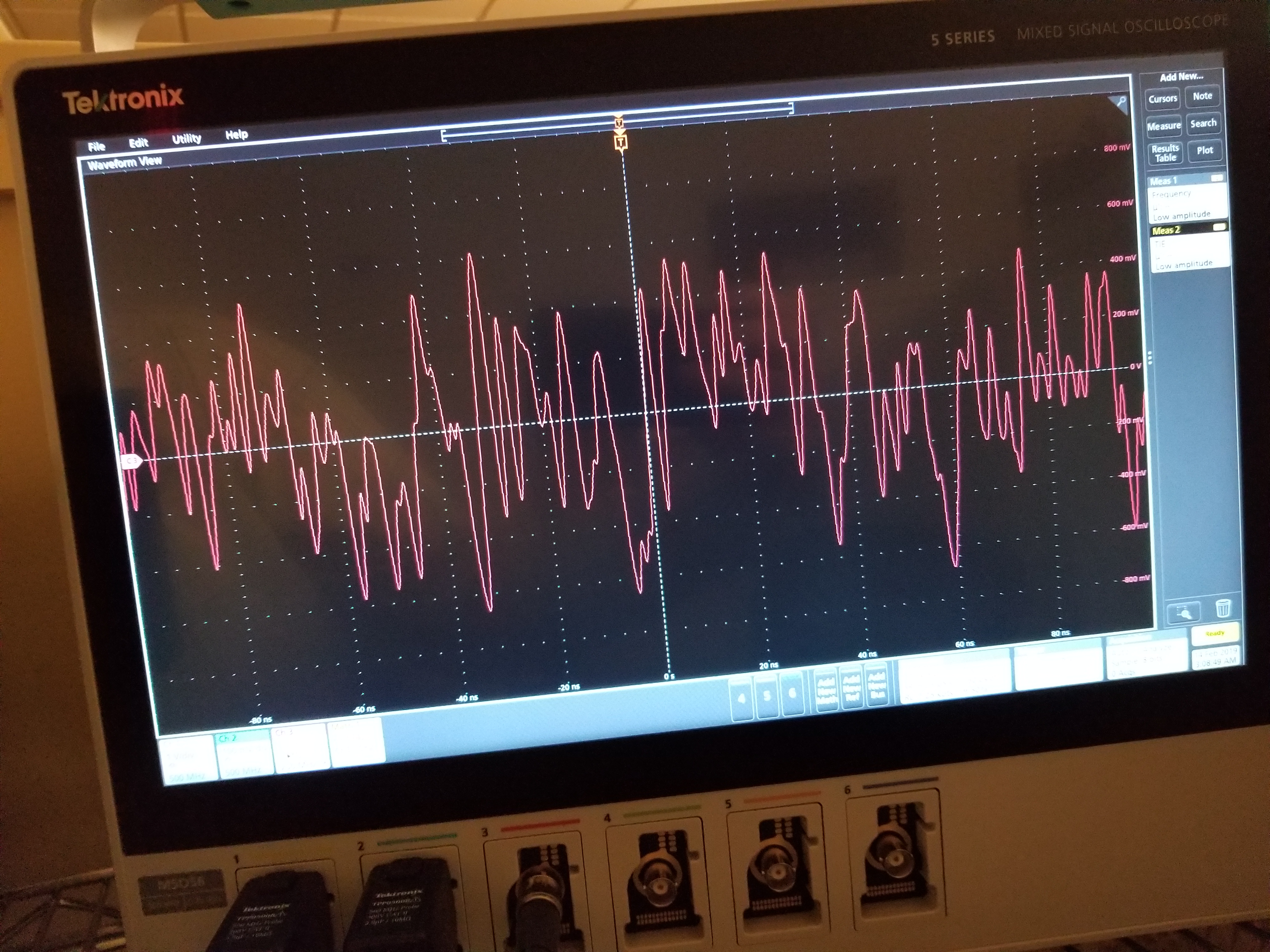
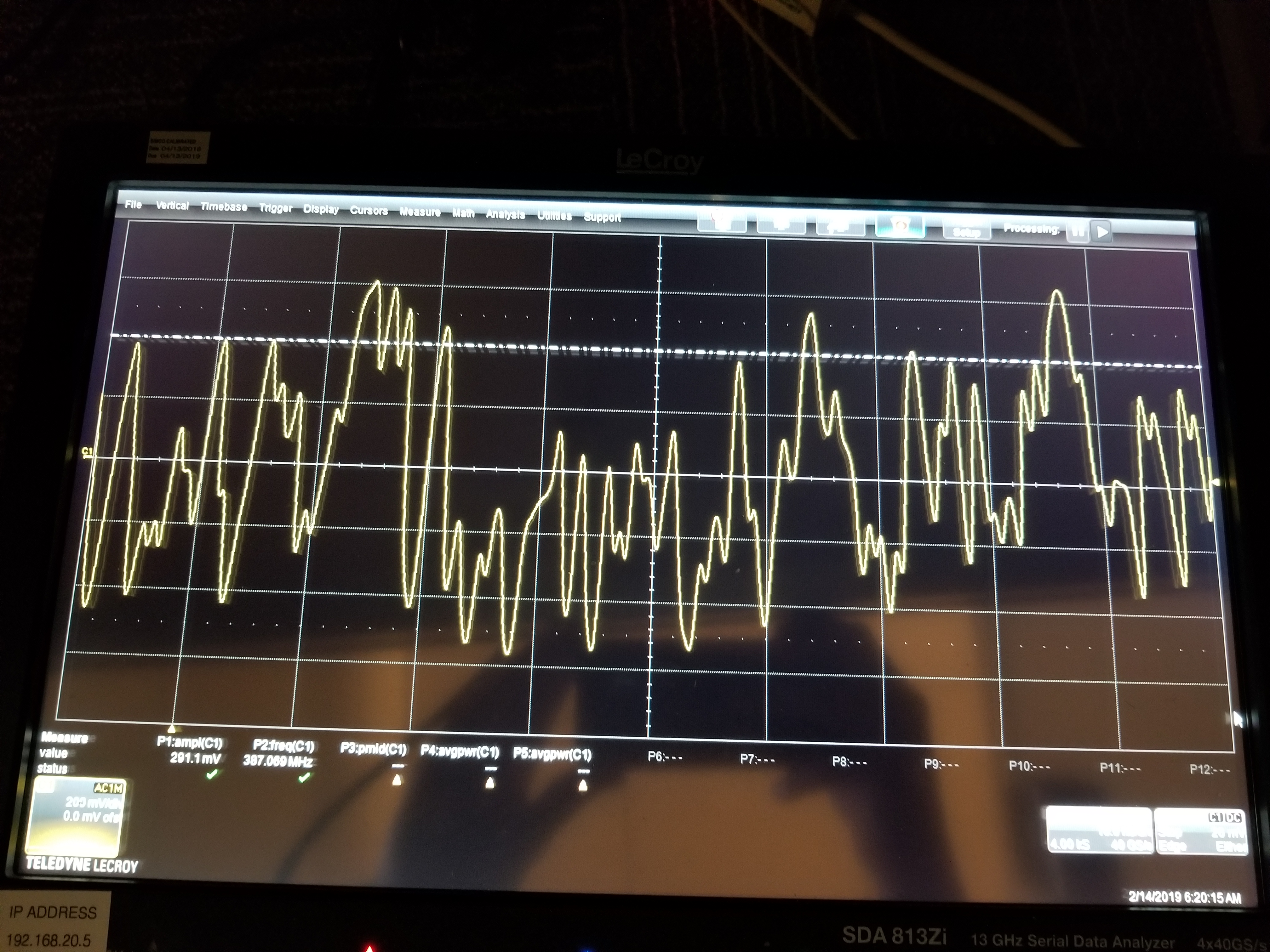
I have a commercial bidirectional HDMI to 3G SDI converter box. If i take this box and hook a computer video output to is and drive the sdi signal into the SD384 eval board and its output into an oscope the eye diagram of the equalized signal is junk. There is too much jitter on the lines and it causes the FPGA to see too many CRCs to recover the signal (when the FPGA is hooked to the receiver instead of the oscope). If i have the FPGA drive signal out to the SD303EVK transmitter board and out the same HDMI to 3G SDI box the signal is recover fine and the image is transitted to an HDMI monitor cleanly. I opened the converter box and found they use a TI part that I cannot find. The chip has the markings: L0604A2 86U AX42. This part seems to recover the 3G SDI signal far better than the LMK384 chip thats on the eval board. What is the difference in these two parts? Why would the LMK384 board be unable to create a clean signal out?
The cable connecting the SDI ports is a 75 Ohm cable and is only 2 feet in length. No where near the hundreds of feet the SDI signal should be able to travel. The same cable is used for both directions so the cable isnt the issue. Also the FPGA has been tried as the source of the HDMI signal (FPGA drive out to the SD384 board then to the SD303 board and the equalized signal is still junk). the FPGA output eye was verified to be very clean and have a very large eye well within spec.
Thanks
Joe