This thread has been locked.

If you have a related question, please click the "Ask a related question" button in the top right corner. The newly created question will be automatically linked to this question.

TCA6424A: TCA6424A doesn't answer on I2C

Part Number: TCA6424A

Dear support team,

I'm trying to get a TCA6424A to work. Sadly, it doesn't reply at all to I2C commands. Another slave on the same bus works without any problems. I would appreciate if you could point me at the thing I'm missing here...

This is a pic of the scope screen:

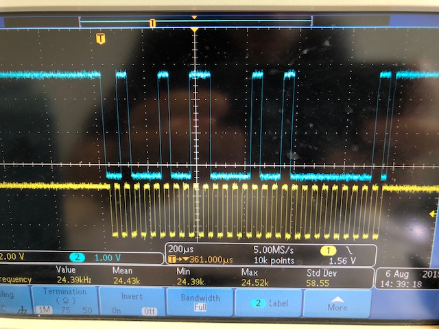
As you can see, the address byte doesn't get ACK'd.

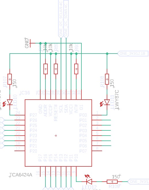
This is the schematic:

As I'm running out of ideas, I'd really appreciate some help here!

Thank you!

Best regards

Lennart

  • Hi Lennart,

    Your schematic looks like a correct implementation of the TCA6424A.  From the schematic and the scope waveforms I gather the following information.  Please correct me if I am wrong.

    Slave address = 0x22

    R/W bit = 0 (Write Mode)

    Command Byte = 0x84 (Register Output Port 0 with Auto Increment)

    Data to Register = 0x00

    SCL frequency = 24.4Khz

    I have duplicated your setup per your schematic with the addition of 4k7 pullup resistors on both SCL and SDA for my setup.  I assume you have pullup resistors on your SCL and SDA lines not shown in your schematic.  In my setup, the TCA6424A acknowledges my I2C bytes with slave address 0x22, command byte 0x84, and data byte 0x00. 

    However, I was able to duplicate your waveforms if I connect the Reset pin to GND (or hold it low) instead of connecting it to VCCI (3.3V).  Since everything else looks to be correct and it should theoretically work, could you double check the Reset pin in your setup to make sure that the voltage on the pin is High (3.3V)?

    If the Reset pin is set correctly and is held high, have you tried other registers, or other TCA6424A devices to rule out a potentially damaged device?  Could there be a possibility of a slave address conflict with another device on the bus?

    Regards,

    Jonathan

  • Dear Jonathan,

    all your assumptions are correct. Please let me add some information:

    - I have 4k7 pullups on SCL and SDA
    - I am driving SCL directly from an FPGA to high or low (ignoring the pullup)
    - SDA is either '0' or high impedance. This seems to work as another chip (Si5344) answers correctly.
    - I am only running this single sequence again and again
    - I took care that after powerup the SDA and SCL lines stay high. The first high-to-low transition on SCL is the one you can see on my scope picture (single shot). Subsequent sequences look exactly the same, though (apart from me toggling the data byte between 0x00 and 0xFF)
    - Reset is bound to 3V3 via a 10k resistor as can be seen from the schematic. I tested with a scope that the reset line is high (it is!).
    - I tried toggling reset using a cable to connect it to GND. Didn't help. (I have to admit though that I am unsure if I really made contact, kinda tricky...)
    - The register number shouldn't play any role since already the address doesn't get ACK'd, right?
    - Since I suspected bad soldering (last resort...), I tried another chip on the same board (different I2C bus). Same result...

    Any other idea? Since I programmed everything in an FPGA, are my start and stop sequences correct?

    Thank you!

    Best regards
    Lennart

  • Hi Lennart,

    I was hoping it was a simple Reset pin issue.  But there are a few things we can still look at.  From your previous waveform, the start and stop sequence look correct.  Also, yes, if the address byte gets NACK'd, then the register number or command byte doesn't matter.

    The first thing is that the Address pin (ADDR) is right between the GND and VCCP pins.  Your desired configuration is to have ADDR = Low.  However, we have seen it in the past that the ADDR pin could be shorted or accidentally connected to the VCCP pin in which case the device will respond to address 0x23 instead of 0x22.  Can you try to check the ADDR pin voltage and try to communicate with it using address 0x23 just in case it is set incorrectly?

    Since you say another device is communicating properly, this one is a long shot, but sometimes the SCL and SDA lines get swapped either on the board or in the MCU or FPGA.  Can you verify that the SCL and SDA waveforms are correct on the actual pins, or by swapping the FPGA pin assignments? 

    And there are always some possible parametric voltage and timing parameter verification we can take a closer look at.  Can you measure the Low and High voltage levels on the SCL and SDA signals?  Your scope shots look clean and they signals appear to be large enough to cross the high and low thresholds, but it is always something to look at.  Then also, do a closer inspection on the clock to data setup and hold times etc.by zooming in on the bits and making the delay measurements.  Preferably this is looked at on the pins of the device but that isn't always possible.  But sometimes it could be possible that there are unexpected propagation delays when the SCL and SDA traces have different lengths on the PCB, or on wires of different lengths if it is a multiple board situation.

    Regards,

    Jonathan

  • Dear Jonathan,

    I am sorry for having bothered you. This is embarrassing, I overlooked the "bottom view" hint in the datasheet, so the control pins are swapped...

    If it doesn't work after the redesign, I'll let you know. Thanks a lot for your help!

    Best regards
    Lennart

  • Hi Lennart,

    You are certainly welcome!  I am sorry to hear about the mixup and I wish you luck on the redesign.  I too have fallen into a similar situation in the past and know it is frustrating.  But thanks for considering and choosing our parts for your design!  Please definitely reach out to us if you have any further questions or need additional support.

    Best Regards,

    Jonathan