This thread has been locked.
If you have a related question, please click the "Ask a related question" button in the top right corner. The newly created question will be automatically linked to this question.
Hi Team ,
my customer is using SN65LVDS93 as solution and have below 2 questions
1. they have been use SN75LVDS84A(21:3) before , now they are using SN65LVDS93(28:4) for new project ,
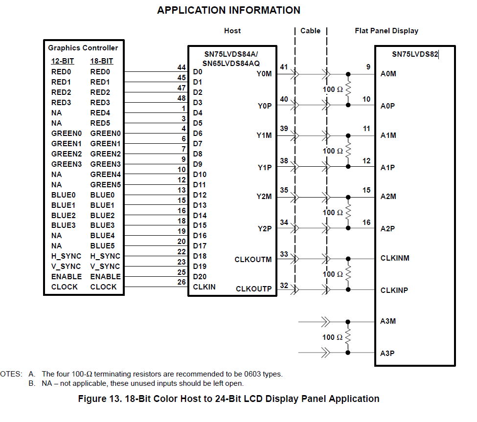
so is the pin D24~D27 is used as below SN75LVDS84A d/s shown? And reference application pic in SN65LVDS93's d/s for my customer reference?
per my assume is yes , SN65LVDS93(28:4) should be same functionality with SN75LVDS84A(21:3) , just with more input .
2. About CLKSEL pin,if customer's Graphics Controller didn't have this pin to connect with ,where's should CLKSEL pin(即第17Pin) connect?
Can it left floating? if yes, in this condition the clock valid is at the rising or falling edge?
please kindly help on the questions above , thanks in advance!
Andy
Could you clarify question 1. With SN65LVDS93, is the customer still going to use the 18bit format or they are moving to use 24bit format?
For question 2, the customer can tie CLKSEL to GND or VDD with a resistor. They don't need to use a dedicated pin from the graphic controller.
Best Regards,
Charley Cai
Hi Charley,
Thanks for the feedback!
For Q1, they are moving to 24 bits application for this new project .
as for Q2, so they can tie CLKSEL to GND or VDD with a resistor , and CLKSEL tie to GND the CLK active is falling edge and VDD for rising edge , right?
Andy
Hi Andy,
1. In this case, the customer should follow SN65LVDS93 datasheet figure 1 to map out the pin connections. This would also depends on the data mapping required by the receiver.
2. Yes, this is correct.
Best Regards,
Charley Cai