Other Parts Discussed in Thread: SN75ALS176B
Hi,
From the following E2E.

Could you please review for the calculation for SN65HVD3080E.
SN65HVD3080E driver side : 60mA(max) >32mA
Receiver side 0.13mA(max) at 12V, -0.1mA(min) at 7V, So, 12V side = 0.13/1=0.13UL and -7V side = 0.1/0.8=0.125UL.
Should they use 0.13UL that is higher one?
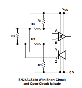
Also, SN65HVD3080E has Failsafe Receiver (Bus Open, Short, Idle) function compare with SN75ALS176B.
SN65HVD3080E don't need the Fail safe circuit like as application note. because input hysteresis is -0.2V to -0.08V. Is it correct?
And, Can it drive 32UL/0.13UL = 246 node for BUS?
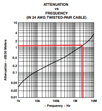
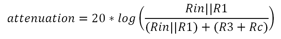
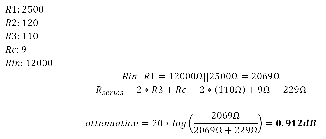
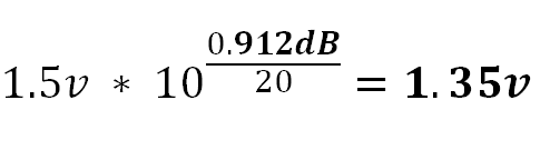
Regarding Attenuation
At they use the bottom circuit of Figure 7 of application note with SN75ALS176B. A=-1dB.
If they use TP cable of Figure 3. Total 4pcs (master, slave) /1Bus.
(Attenuation allowed in transmission line) = -6 - (-1)x4 = -2dB
From figure3, they can use until 5Mbps, 30m.
From figure3, If they want to use 100m cable, they can use until 650kbps, 100m.
Is it correct?
Thanks
Muk