This thread has been locked.

If you have a related question, please click the "Ask a related question" button in the top right corner. The newly created question will be automatically linked to this question.

TCAN334: Glitch on VID for receiver

Part Number: TCAN334

Hi Team,

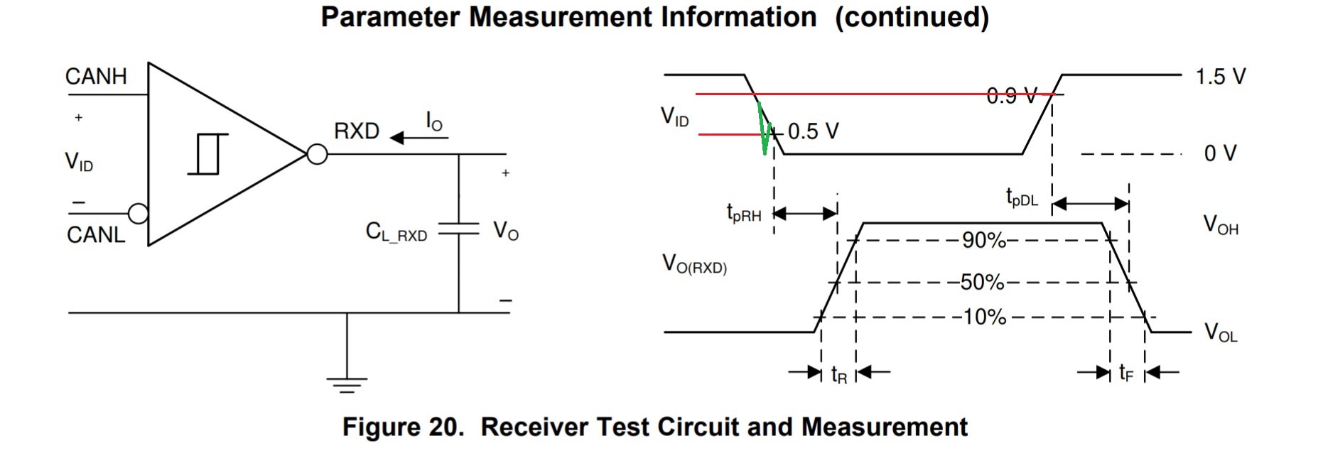
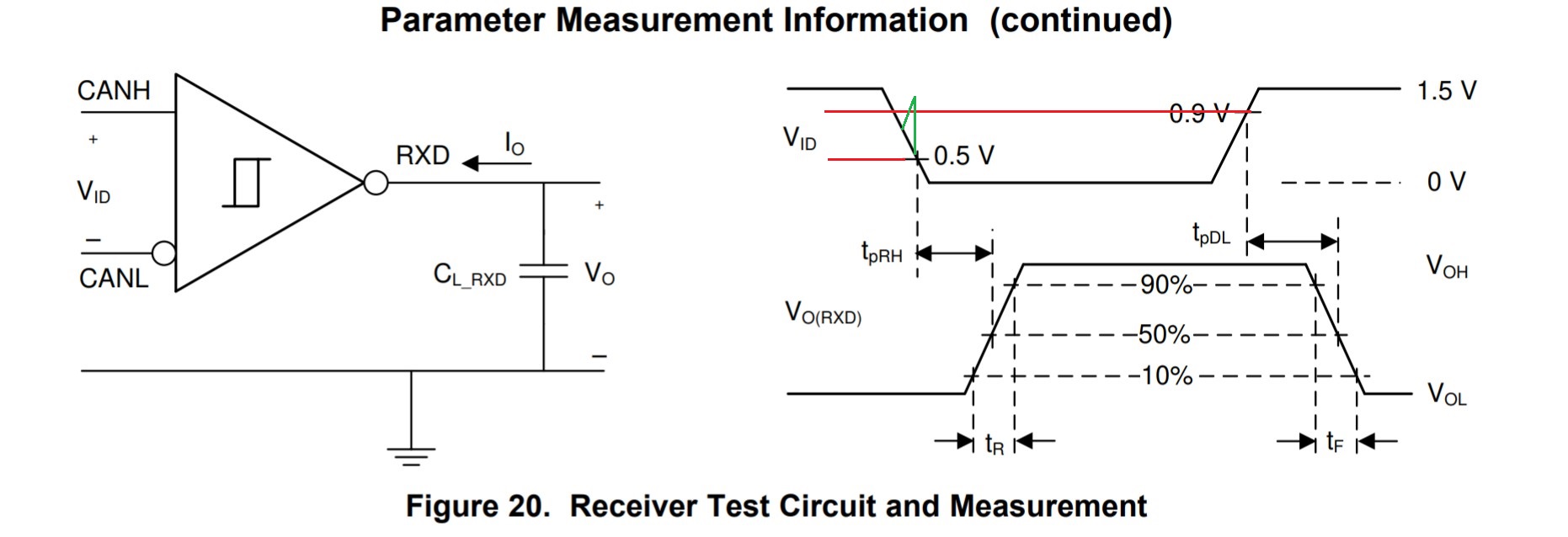
When TCAN334 is for receiver, if there is glitch on VID and the glitch voltage is between 0.5V and 0.9V shown in picture below, will the Vo(RXD) keep the same without change?

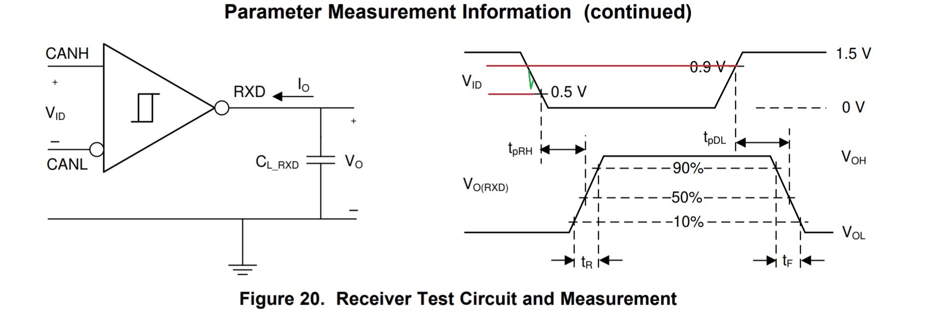
If the glitch voltage is below 0.5V or above 0.9V shown in picture below, may I know:

1. Will the Vo(RXD) change?

2. If the answer for item is yes, what's the minimum time requirement for the glitch voltage below 0.5V or above 0.9V?


Thanks and Best Regards!

Hao

  • Hi Hao,

    This is an interesting question. To better understand how these conditions relate to some datasheet values, let's first look at how the receiver operates and then we'll take a look at theoretical timings.

    The ISO 11898-2 standard specifies that all bus differential states below 500mV shall be interpreted as recessive and all states above 900mV shall be interpreted as dominant. This is described in TCAN334's datasheet as receiver input thresholds. Let's assume our actual positive threshold value for switching is in the middle of this range at 700mV. The datasheet also defines a hysteresis value of 120mV. This means in our theoretical receiver, when the differential rises past 700mV the receiver registers a dominant state - and when the differential falls below 580mV the receiver registers a recessive state (Note that these values are used as an example and actual values may vary).  For the positive glitch that you describe to occur, the differential Vid would have to rise above our Vth+ of 700mV and then fall to less than Vth- of 580mV in time Tglitch. Conditions which allow the bus differential to linger in this indeterminate zone (500mV < Vid < 900mV) should be avoided to maintain noise immunity. If this cannot be done, the receiver would be susceptible to noise spikes.

    Assuming TCAN334 was exposed to conditions as described above, we can theorize how the RXD pin will react at different Tglitch timings. First, if we assume Tglitch > tpRH or Tglitch > tpDL, we can expect a pulse to occur on the RXD line which is proportional to the glitch seen on the receiver inputs. In this case, the glitch is longer than the time it takes the signal to propagate through the device to the RXD line. Looking at the opposite end, if Tglitch < tR or Tglitch < tF, then we would expect to see minimal if any distortion on RXD. This is because the receiver won’t react fast enough to change the pin state before the glitch has reverted.

    what's the minimum time requirement for the glitch…

    There are two potential answers to your question. The first is that glitches on Vid with pulse-width less than the rise/fall-time of the receiver will likely not affect the perceived RXD state. The second is that the pin state on RXD is only relevant to a CAN controller during the sample point (in most cases). This means that a potential glitch that does propagate through TCAN334 would have to fall directly on this sample point to impact the received data by the controller. Lastly I will reiterate that the bus should not be left hanging in this intermediate potential between 500mV and 900mV. If far enough outside of this range, the system will be immune to low-level noise that could cause the glitch you describe.

    Let me know if this explanation makes sense and if you have any more questions.

    Regards,
    Eric


  • Hi Eric,

    Thanks for the detailed explanation.

    Best Regards!

    Hao