This thread has been locked.

If you have a related question, please click the "Ask a related question" button in the top right corner. The newly created question will be automatically linked to this question.

DP83822EVM: Problems configuring the PHY in RMII Mode

Part Number: DP83822EVM

Hello,

I am testing the RMII mode with my external MAC.

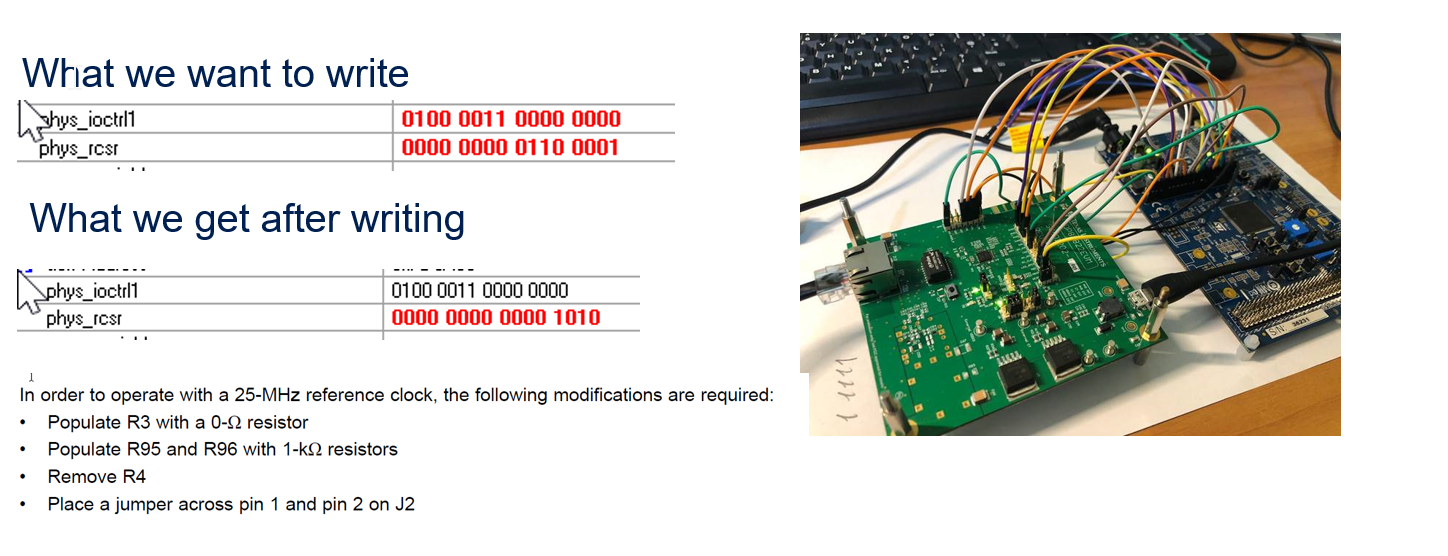
I followed everything I think should be followed in order to enable RMII, but I cannot manage writing RSCR correctly.

Phy is working in master mode with 25MHz clock.

The only point I don't see compliant is the value of R3: in the board I got 18Ohm. I think it was put on purpose and maybe the shortage is in necessary.

I think we are missing something.

thanks in advance for your support.

Regards

GZ

  • Hi Giulio,

    I am not sure which register you are referring to for phys_rcsr. Can you tell me which register number you are reading from the register map of the datasheet? 

    Are you also ensuring that you have strapped correctly per the datasheet recommendations? You can read back register 0x467 to confirm this. 

    Thanks,

    Cecilia

  • Ciao Cecilia,

    The register are:

    IOCTRL1: 0x0462  <-- accessed in RW via extended registers operations

    RCSR: 0x0017 <-- accessed in rw via regular MDIO RW operations

    The board has not strap  options  configurable by jumpers  so I tried to reconfigure the board itself by writing those registers.

    Thanks.

    G

  • Please Meanwhile can you tell me exactly the sequence I am supposed to follow in order to enable RMII?

    Regards

  • Ciao Cecilia,

    I can confirm that watherver I do I cannot  configure the following

    registers 0x017 [RSCR] --> that in my understanding should be 0x20/0x21 (regular MDI write operation)

    and 0x0462 [IOCTRL1] --> that should be 0x4300 (exrtended MDI writ eoperation) as suggested in the datasheet.

    I also tried with an external strap on RX_DV in order to set it tom mode 3. for the purpose  (I don't have 0402 resistors) I exploited  a standard through voltage divider with 5.6K Pullup and 2.4K PD.

    5.6K end to a free 3.3V pin in connector J6

    the center tap to RX_DV

    the  2.4K free end to the gnd line on K14.

    As soon as I do that the phy registers are read as FF and even SOR1 and SOR2 are completely wrong.

    If I remove this trivial voltage divider straps and phy regs are read correctly but I cannot set bit 5 in RSCR.

    I also reassembled the two board with shorted wires, the most delicate  were directly soldered between the two boards.

    I don't know what else to do without your support.

    regards,

    G

  • Hi G

    Thanks for the updates. When you say that you are 'getting different values after writing' are you saying that they are not the expected register write settings you wrote in, and in fact you are reading the incorrect bits? 

    Can you confirm if you try writing other registers that you are seeing the expected register writes for other addresses? Can you also provide the MDC frequency you are using when reading/writing registers?

    The typical steps through register writes to enable RMII include only writing to 0x0017. All you need to do is write to bit 5 to enable RMII mode as well as writing to bit 7 for the correct clock reference. That is our typical setup for register writing to these modes.  

    Thanks,

    Cecilia

  • ciao Cecilia,

    As you requested I measured the MDIO activity during the writing of register 0x17 bit 5.

    The stack I am using is proved working, we've been using It in MII with no problems whatsoever. the MDI frequency Is at about 1MHz and I am positive about read and write for all the other registers as you can see from the register dump I sent you before.

    In this trial I found 5 set  ( neve happened before) but Register 0x0462 is completely wrong.

    The 50MHz master clock is expected to be routed via RX_D3, so the configuration of register 0x462 should be  0x4300, right?

    If I try to write  0x4300 to this register I get 0x099F.

    I put as a reference for you the content of SOR1 (0x0467) and SOR2 (0x0468) s a proof that the access procedure for the extended registers is correct.

    The board , as I pointed out  before,  is configured with the phys in master mode, so it is fed with 25MHz from PLL (with J12 in default position) .

    Thanks

    G


  • Ciao Cecilia,

    could you give me example code to use RMII and 50MHz internal clock for the EVM board?

    Regards

    Giulio

  • Hi Giulio,

    Do you mean 1MHz clock on MDC no MDI? If yes, then that should be ok for MDC frequency.

    Example code for the EVM would be to read back register 0x17. You can then use that and only change bit [7] = 0 for 25MHz reference clock and bit [5] = 1 to enable RMII mode. 

    You should then see the 50MHz on RX_D3. 

    Can you confirm you see RX_D3 on this pin when you configure these registers? 

    Thanks,

    Cecilia

  • Ciao Cecilia,

    Yesterday we could finally get a working ping. For that we also had to write 0x4300 to register IOCTRL (0x0462) in order to enable the master clock via RX_D3.

    It was important to solder all the delicate signals with short wires. I also had to move MDIO and MDC wires away from the RMII clock in order to avoid interference.

    I noticed that, after a while the device stops working  if there were some internal reset that restores the device to MII mode (RX_D3 stops outputting the clock). I'll be investigating this issue too.

     Any idea about what might be the cause of that?

    Regards,

    G

  • Hi G

    I am glad you were able to get the ping working. Can you describe in more detail about when the device stops working? Is it while data transfer is occurring? I am wondering if it is because of the soldering and some of the delicate signals interfering with the reset.

    Thanks,

    Cecilia

  • Ciao Cecilia, sorry for the delay but I am currently on vacation.

    What I saw is thatn at a certain point during the ping, the device stopped replying. In this condition I could verify that the device somehow reverted back to MII mode because the clock in RXD_3 was missing ( instead there was the classic data shaped transaction).

    I'll be futher watching the problem as soon as I get back to work, next week, but I don't think the problem is related to the FW.

    Regards,

    G

  • Hi G,

    That is an interesting phenomenon. Please share your test results when you find out. I am wondering what is driving the device to reset back to MII and if is occurring at the same points.

    Thanks,

    Cecilia