This thread has been locked.

If you have a related question, please click the "Ask a related question" button in the top right corner. The newly created question will be automatically linked to this question.

SN65LBC180-Q1: Output Voltage Range

Part Number: SN65LBC180-Q1

Hello team,

My customer has a question for output voltage range of SN65LBC180-Q1. Can you provide us the below information?

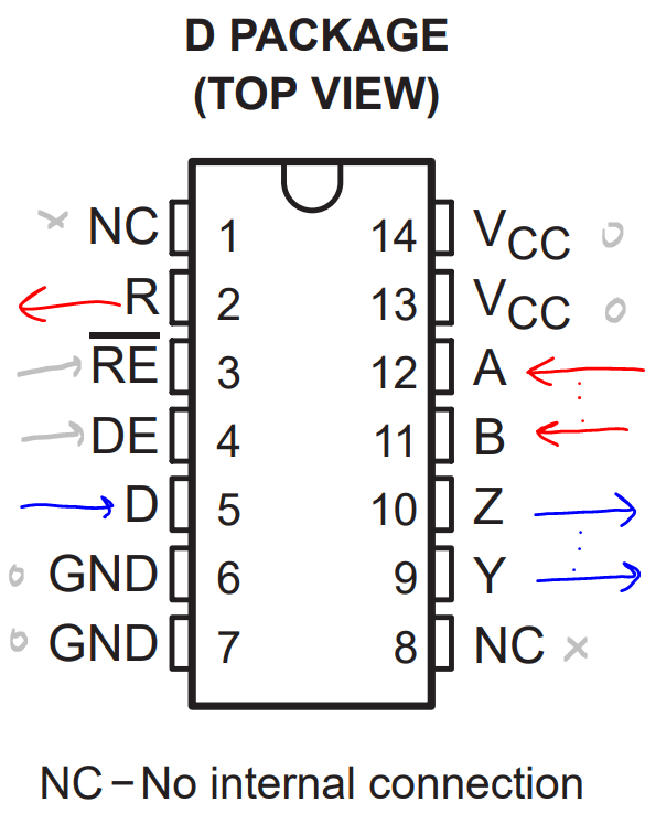
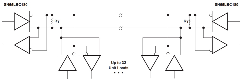
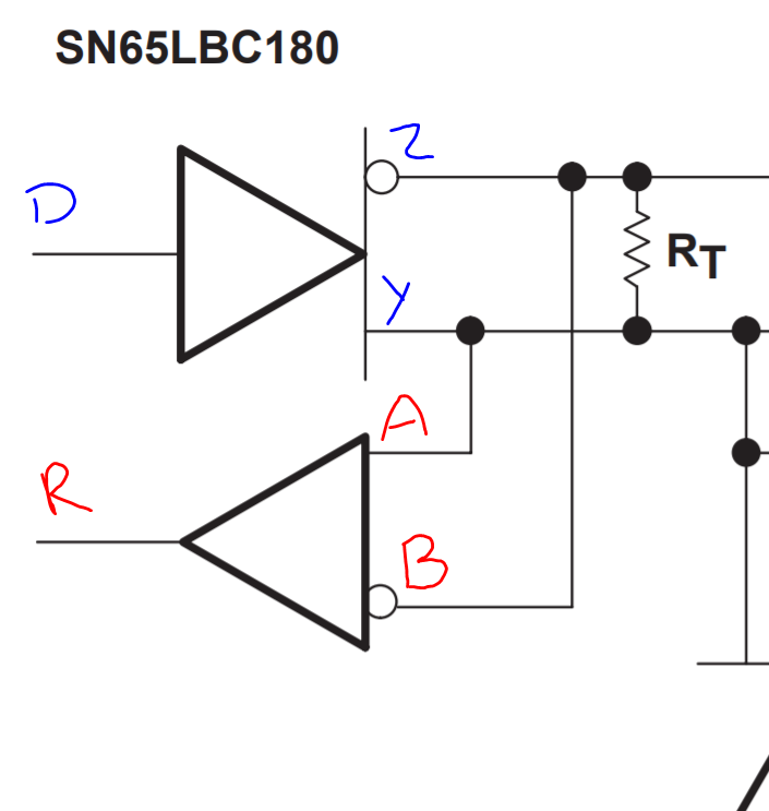
When VCC = 5V, D = 3.3V is input, please tell us the normal output voltage range (min ~ max) of the A, B, Y, Z, R terminals.

Best regards,

Shotaro

  • Hi Sakai-san,

    The output level will depend on the loading.

    Fig-8 & Fig-14 provide an overview of Voh vs. Ioh for Vcc=5V

  • Sakai-san,

    Thanks for reaching out. Not all of the pins out listed are output pins. I hope this drawing I made helps visualize the data/logic flow across this device:

    Ravi is absolutely correct. Figure 8 and Figure 14 provide overviews of the change in high-level output voltage for the driver and receiver respectively across different output current loads. Here is some additional information using only the “typical” values listed on the datasheet’s electrical characteristics sections:

    Output differential voltage VOD = VY – VZ

    When D (“Driver”) is high at 3.3V, you can expect an output of High at Y and Low at Z. This would give a positive VOD. According to the datasheet, you can expect a typical VOD of 2 V with 60 Ω termination RL (and a typical VOD of 2.5 V with 54 Ω termination RL). Since this device has a typical common-mode voltage of 2.5 V, you can expect VY around 3.5 V and VZ around 1.5 V. Keep in mind, however, that the figure of merit is differential voltage VOD.

    According to my estimations:

    VCC

    RL

    D (in)

    Y (out)

    Z (out)

    VOD = Y – Z

    5 V

    54 Ω

    3.3 V

    3.75 V

    1.25 V

    2.5 V

    5 V

    54 Ω

    0 V

    1.25 V

    3.75 V

    -2.5 V

    5 V

    60 Ω

    3.3 V

    3.5 V

    1.5 V

    2 V

    5 V

    60 Ω

    0 V

    1.5 V

    3.5 V

    -2 V


    Input differential voltage VID = VA – VB

    The output at R (“Receiver”) is determined only by the input differential voltage VID. The voltages at A or B are not independently relevant to the output at R – just the difference between the two (provided the absolute maximum conditions of the device are satisfied). Thus, you can use the logic table on the datasheet along with the receiver electrical characteristics to determine its behavior:

    VCC

    VID (in)

    R (out)

    5 V

    VID ≥ 0.2 V

    4.5 V

    5 V

    0.2 V ≥ VID ≥ -0.2 V

    ???

    5 V

    -0.2 V ≥ VID

    0.3 V


    I hope this helps. Let me know if you have any further questions.

    Best,

    Danny

  • Danny-san,

    Thank you for the information. It's very helpful for me.

    The customer considers that when power is applied, a constant voltage is generated even at the input terminal.

    He wants to know the voltage range from min to max. (What is the voltage range of A and B, which are the input terminals?)

    The condition is VCC = 5V, D = 3.3V.

    Best regards,

    Shotaro

  • Sakai-san,

    Great to hear from you. I believe I see what your customer is asking. Let me know if I misunderstand.

    “The customer considers that when power is applied, a constant voltage is generated even at the input terminal.”

    Even though A and B are input terminals, they may present a resting voltage when the device is powered and nothing is connected to the bus. Page 3 of the datasheet shows some schematics of the inputs and outputs. My [very quick and rough] estimation is that the customer may be seeing at least 30% of VCC on A and B when the device is powered but these pins are left floating. Note that, in normal operation, these pins would not be left unconnected/floating.

    “He wants to know the voltage range from min to max. (What is the voltage range of A and B, which are the input terminals?)”

    If your customer is asking what the absolute maximum and minimum permissible values are for A and B, along with the other pins, the answer is that the pins can sustain between -10 V and +15 V with respect to GND before the device is expected to sustain damage. For proper operation, however, these are the recommended conditions:

    • Voltage at any individual terminal A, B, Y, Z should remain between -7 V and 12 V with respect to GND.
    • Differential input voltage between A and B (VID) should remain between -6 V and 6 V.
    • Voltage at D, R, DE, RE should range from GND to VCC. “Low” inputs should range from GND to 0.8 V, while “high” inputs should range from 2 V to VCC.

    Please let me know if I can help in any other way regarding this device’s operation.

    Best,

    Danny

  • Danny-san,

    Thank you for many comments.

    The customer measured the voltage of A and B with Vcc=5V and D=3.3V. A and B is 2.5V and 1.4V, respectively.

    The voltage of A exceeds 30% of Vcc. Is this no problem?

    Best regards,

    Shotaro

  • Sakai-san,

    You're correct. This is no issue. Just keep in mind that these pins are intended to be used as inputs, so the voltage generated when these pins are left open is irrelevant to their normal operation. Here is a typical application of this device:

    Note that these transmission line pins are not left floating in application.

    Regarding your 30% question, this is entirely expected. My brain neglected to account for the threshold voltages of the diodes in the equivalent schematics, so an open-circuit voltage of greater than 30% is completely expected and totally fine. I have updated my prior post to reflect this correctly.

    Best,

    Danny