A related question is a question created from another question. When the related question is created, it will be automatically linked to the original question.
If you have a related question, please click the "Ask a related question" button in the top right corner. The newly created question will be automatically linked to this question.
LMH6525: schematic review including non-use pin condition
The customer looks like they are aiming for around 400mA of total output current. For pin 9 (I2 Channel 2 Current Setting), the datasheet states that the maximum output current is 300mA. It seems like they are expecting 407mA of channel current which will not be possible. I calculated a total of 309mA output current from Read Channel and Channel 2 combined. If the customer needs more than 309mA, I would advise lowering resistance of IR or using channels I3 and I4. Customer also did not show these pins (I3 and I4 which are pins 10 and 11), would they be able to provide connections to those pins?
For the oscillator frequency connections (pins 12-15), the datasheet states this should be set using an external resistor to ground. If they want the minimal amount of frequency/amplitude, I would suggest placing a very high resistance to ground. From the PDF you provided, the enable pins (ENOSC and ENOSCB) are set to be enabled, so the oscillator will be used. If they want to use this feature, I would advise checking datasheet pages 11 and end of page 12 and set according to their desired amplitude and frequency.
Lastly, I had a question on why the customer is enabling channel B pins when SELB is set to low. This will only increase supply/quiescent current. Also according to the highlighted row in table 2 Iout control in the pdf. They want EN3 and EN4 disabled, however they are set to high in the schematic.
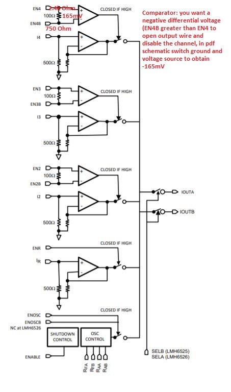
Thank you for the updated schematic. The connections look good, but I believe the customer has EN4 and EN4B voltage source/gnd flipped. I have attached an image below with notes on how to disable the 4th channel. I found the block diagram of the LMH6525 on page 9 of the datasheet. Let me know if you have questions on this. For the DS90C031BTM connection, it looks like the specs in the datasheet were tested with a resistive load of 100, which would fit in this case in regards with the block diagram for the LMH6525. To enable these channels, Dout+ needs to be greater than Dout- for each respective channel (2 and 3).