I am new to USB 3.0. How much on-board matching an iterative changes to trace geometry are required? Is it a case where if you conservatively follow the layout guidelines, you can pass on your first attempt?
I have worked with 5GHz RF traces and impedance matching with a VNA, but my experience with high-speed digital islimited to the 400Mbs range. I don't have a feel for how sensitive 5 Gbps is to subtleties in layout. Do people typically use special materials like Rogers with lower dielectric constants or can you use normal FR-4-like substrates?
Do you typically need a scope fast enough to see the eye diagram at 5 Gbps?
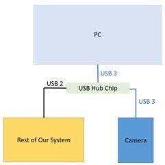
Fortunately, the interface on my board is 12Mbps USB. The Hub chip would only be moving data. It could be kept close to the connectors. But at 5Gbps, one inch of trace is about one bit period, which feels staggeringly fast to me.