


Hi Team,
I am seeking clarification on the N.C. pins of the TPD4E05U06-Q1. I realize these pins are to allow the signal traces to be straight through routing, but it is unclear 1) how they should be wired on the schematic and 2) the how they should be connected on the PCB
For number (1), you mention in the pin description:

But then in the application example, instead of not connecting anything to these pins, they are wired up:

Therefore, if I want to use these "no connect" pins for straight wire routing, should they actually be connected to the signal lines (in that case, they shouldn't be considered no connect pins).
For number (2), in the actual layout, it appears the signal goes underneath the pad of the pins, but I cannot tell if the signal is actually electrically connected to the pins? Should these pins be physically connected to the signal traces? If so, that again doesn't correspond to a "no connect" pin..
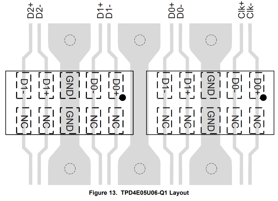
If the signals are not to be electrically connected to theses pins, and the signals are on the top layer, should there be a mask between these pins and the traces so they are guaranteed to not be connected? That would contradict the schematic though..
I appreciate your insight.
-Jared

