This thread has been locked.

If you have a related question, please click the "Ask a related question" button in the top right corner. The newly created question will be automatically linked to this question.

TCA9545A: how to measure Vpass

Part Number: TCA9545A
Other Parts Discussed in Thread: TCA9554, TCA9554A

Dear Expert,

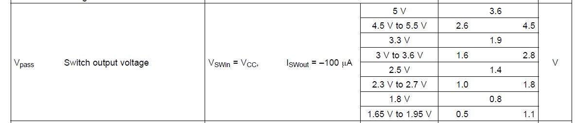
I'm confused by the Vpass parameter. the TCA9545A shows that.

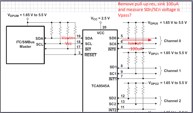
what does Vswin and Iswout means?  i try to config my bench as below figure ,does it right ? given Vcc at SDA and sink 100uA at SDn, thern measure the voltage is Vpass?

  • Hi Hui,

    To measure 'V pass' you need to:

    • enable a channel (lets assume channel 0)
    • Apply Vcc SDA/SCL
    • pull 100uA from ch 0 (use a resistor with an ammeter to ensure you get 100uA)
    • Look at the voltage at Ch 0

    This basically tell you the Vth of the pass FET.

    -Bobby

  • Hi bobby, thanks for reply

    Then Vth equals to (Vcc-Vpass), right ? it seems Vpass is indepent of Vswin shows on the datasheet,

    and why we specify 100uA but not other value,  for example, if we pull 200uA, Vpass changed ?

  • In my opinion, I take TCA9545 as a NFET as below,the gate voltage is VCC(determine Vpass=VCC-Vth),one side with VDPUM, the other with VDPU0-3

    datasheet says "Vpss equal to or lower than VDPUX",which means when we transfer '0' NFEF is ON, when we transfer '1', NFEF is OFF, is it right ?

  • Hui Zhang28 said:

    In my opinion, I take TCA9545 as a NFET as below,the gate voltage is VCC(determine Vpass=VCC-Vth),one side with VDPUM, the other with VDPU0-3

    datasheet says "Vpss equal to or lower than VDPUX",which means when we transfer '0' NFEF is ON, when we transfer '1', NFEF is OFF, is it right ?

    [Bobby] Yes, correct. The NFET you drew below has its body substrate tied to GND instead of either of the source/drain to stop the device from backbiasing a parasitic diode. So either side of the FET can be the source interchangeably.

    "Then Vth equals to (Vcc-Vpass), right ? it seems Vpass is indepent of Vswin shows on the datasheet,

    and why we specify 100uA but not other value,  for example, if we pull 200uA, Vpass changed ?"

    [Bobby] We use the 100uA value to have a similar comparison with our competitor (they were first to market with their device, we released after them). I suspect the of current isn't that important since we are acting in the linear mode of operation for the FET. As you pull more current you will eventually saturate the FET and the current will clamp, so a lower current value is used.


    -Bobby

  • "Vpss equal to or lower than VDPUX", does it means, for Vpass , the lower , the better ?

    Another similar question about Switch on-state resistance, how to measure it?

    1.enable the SDn/SCn

    2.sink 15mA on the downstream pair and make Vo=400mV, mesure voltage on the upstream Vi

    3. Ron=(Vi-400)/15, right ?

    Sorry to ask so many questions

  • PS: for IOL of SDA, "6.5 Electrical Characteristics" shows when VOL=0.4, TYP IOL=7mA, but Figure1 shows IOL=8mA @1.65V, much larger @ 3.3V and 5.5V....

    Is there any mistakes?  which data is more accurate

  • About TCA9545A  “Figure21. Glitch Width and height“, the VCC_GH is absolutely value, different with TCA9554 VCC_GH is the drop referd to VCC. which one is right?  

    case 1, "VCC_GH=1.2V when VCC_GW=1us",  Does it means if VCC=5.0V,  VCC_GH=1.5 when VCC_GW=1us, TCA9545A will be reset ?

    case 2, "VCC_GW=10us when VCC_CH=0.5*VCC will not cause a functional disruption" ,  when VCC>2.4V, VCC_GH>1.2V, reset or not reset ?

    case 3, for TCA9554A, if VCC_MV=1.5 but VCC_GH is violated, TCA9554A reset or not reset ?

    -ZH

  • Hui Zhang28 said:

    "Vpss equal to or lower than VDPUX", does it means, for Vpass , the lower , the better ?

    [Bobby] No, this just means that Vpass is defined as the lowest voltage on the main/secondary channel so that u can pick Vcc accordingly (based on figure 17). Lower doesn't mean better or worse.

    Another similar question about Switch on-state resistance, how to measure it?

    1.enable the SDn/SCn

    2.sink 15mA on the downstream pair and make Vo=400mV, mesure voltage on the upstream Vi

    3. Ron=(Vi-400)/15, right ?

    [Bobby] I imagine you may need to place a small resistor before the SDA/SCL and after SDn/SCn and adjust the resistance such that you pull 15mA/10mA while the Vo (seen by the SDn/SCn is 0.4V while SDA/SCL is tied to Vcc through that small resistor). Then you would take the voltage drop across the channel and divide by 15mA/10mA.

    Sorry to ask so many questions

    "PS: for IOL of SDA, "6.5 Electrical Characteristics" shows when VOL=0.4, TYP IOL=7mA, but Figure1 shows IOL=8mA @1.65V, much larger @ 3.3V and 5.5V...."

    [Bobby] I would use the one in the electrical characteristics (section 6.5) since it gives a worse value (likely for margin). The IoL becoming better as Vcc increases makes sense. You can see in the figure that at 1.65V, the current begins to start clamping at around 11mA as the pass FET begins to enter saturation. when you increase Vcc (the gate voltage) the saturation voltage becomes larger so IoL gets pulled lower for a given VoL.

    "About TCA9545A  “Figure21. Glitch Width and height“, the VCC_GH is absolutely value, different with TCA9554 VCC_GH is the drop referd to VCC. which one is right?  

    [Bobby] This is likely a typo, the datasheet should say TCA9545A.

    case 1, "VCC_GH=1.2V when VCC_GW=1us",  Does it means if VCC=5.0V,  VCC_GH=1.5 when VCC_GW=1us, TCA9545A will be reset ?

    [Bobby] If you have a brownout situation where Vcc drops below 1.2V for longer than 1 uS, then when it gets pulled back to 5V the internal registers may have changed to a non default value. (possible reset).

    case 2, "VCC_GW=10us when VCC_CH=0.5*VCC will not cause a functional disruption" ,  when VCC>2.4V, VCC_GH>1.2V, reset or not reset ?

    [Bobby] If Vcc doesn't move but Vcc_channel dips below 1.2V, nothing happens to the device in terms of reset (No reset occurs).

    case 3, for TCA9554A, if VCC_MV=1.5 but VCC_GH is violated, TCA9554A reset or not reset ?"

    For the TCA9554A datasheet (different than the original topic of discussion), I think the values need to be swapped based on figure 32. Vcc_GH should be 1.5V max and Vcc_MV should be 1.2V min. At 1.5V for this device, no glitch/reset is expected. (Otherwise the figure needs to be switched instead because currently they do not match with the table).


    -Bobby

  • [Bobby] This is likely a typo, the datasheet should say TCA9545A.

    Do you mean TCA9545 is right, and VCC_GH is the absolutely value of VCC but not the dips height, Sure ?

    [Bobby]a non default value. (possible reset).

    if reset , why a non default value ? should it be default value

    [Bobby] If Vcc doesn't move but Vcc_channel dips below 1.2V, nothing happens to the device in terms of reset (No reset occurs)

    Why no reset occurs? 


    in my opinion, if there is a  glitch on VCC( VCC_GH or VCC_GW is violated), there will be reset occurs  like POR.