This thread has been locked.

If you have a related question, please click the "Ask a related question" button in the top right corner. The newly created question will be automatically linked to this question.

DP83TC811R-Q1: Ping can't work

Part Number: DP83TC811R-Q1
Other Parts Discussed in Thread: TDA2E

Dear team,

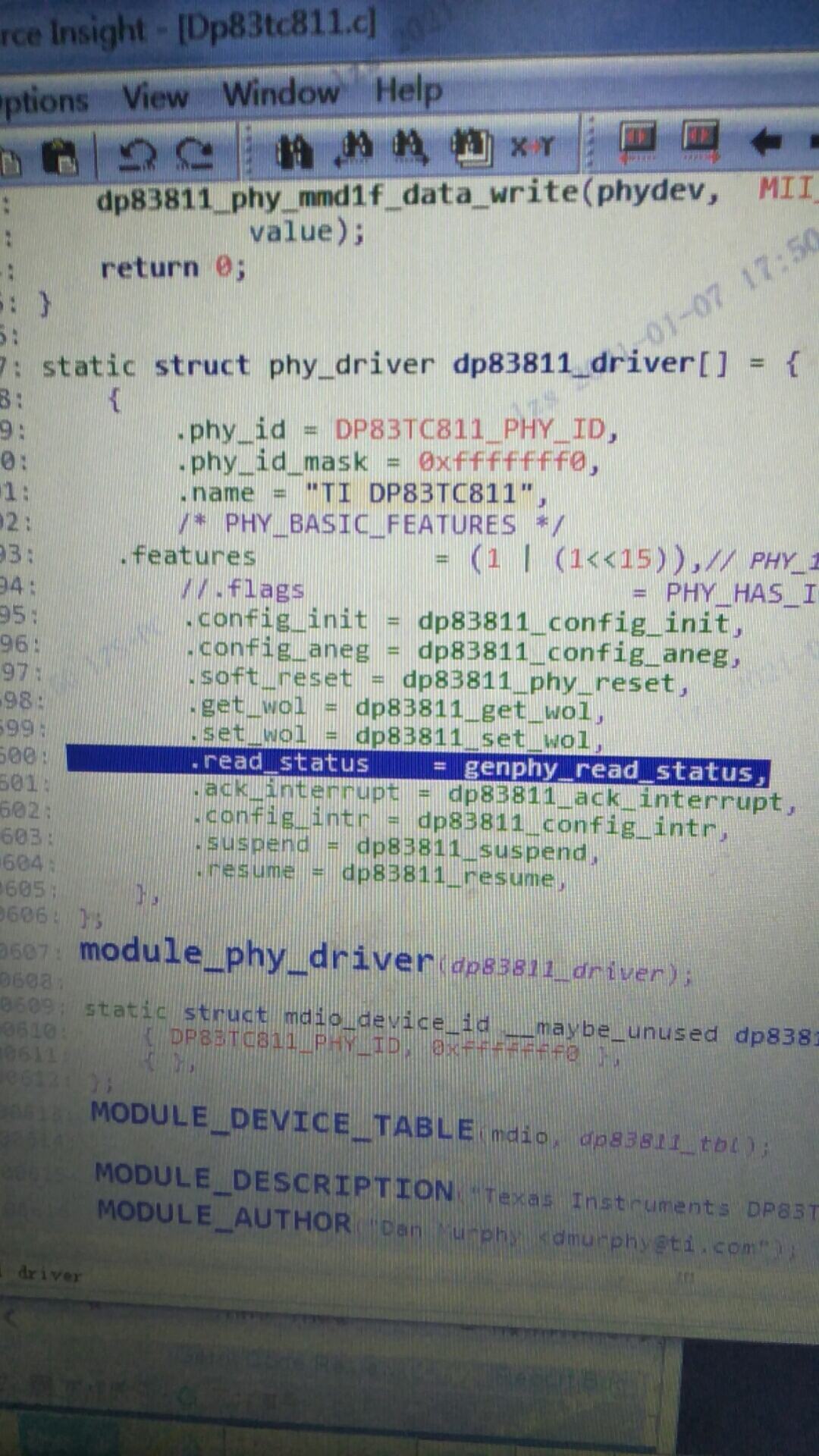
My customer use DP83TC811R-Q1, RGMII, and the SOC is TDA2E. Currently based on our linux driver code as below link, they can read and write 811's registers, but Ping can't work, and at the same time, 811's 0x1 registers indicates no link. Could you please help analyze this issue?

driver code:https://git.kernel.org/pub/scm/linux/kernel/git/torvalds/linux.git/tree/drivers/net/phy/dp83tc811.c

In my understanding, I just need to change the first line to ''#define MII_DP83811_RGMII_CTRL 0x017'', right?

Do we need to configure other registers of 811?

Thanks & Best Regards,

Sherry

  • Hi Sherry,

    There should be no changed needed to the linux driver to be able to establish link. Can you describe how you are configuring the DUT and its link partner? Please also provide the register information for registers 0x00-0x1F, 0x467. 

    Regards,
    Justin 

  • Hi Justin,

    We have some progress today. We find read status in the driver code doesn't achieve, after customer achieve it, the link is normal. But Ping still can't work.

    registers dump is as below:0x00-0x1F, 0x467

    [ 59.248525] ##### att_show read reg = 0x0,value = 0x2100
    [ 59.252684] ##### att_show read reg = 0x1,value = 0x61
    [ 59.261002] ##### att_show read reg = 0x2,value = 0x2000
    [ 59.268803] ##### att_show read reg = 0x3,value = 0xa253
    [ 59.277651] ##### att_show read reg = 0x4,value = 0x1
    [ 59.283381] ##### att_show read reg = 0x5,value = 0x0
    [ 59.290147] ##### att_show read reg = 0x6,value = 0x0
    [ 59.297753] ##### att_show read reg = 0x7,value = 0x2001
    [ 59.301559] ##### att_show read reg = 0x8,value = 0x0
    [ 59.312866] ##### att_show read reg = 0x9,value = 0x2000
    [ 59.319761] ##### att_show read reg = 0xa,value = 0x100
    [ 59.327562] ##### att_show read reg = 0xb,value = 0x1000
    [ 59.334832] ##### att_show read reg = 0xc,value = 0x0
    [ 59.344061] ##### att_show read reg = 0xd,value = 0x401f
    [ 59.349921] ##### att_show read reg = 0xe,value = 0x0
    [ 59.356681] ##### att_show read reg = 0xf,value = 0x0
    [ 59.362923] ##### att_show read reg = 0x10,value = 0x1084
    [ 59.369681] ##### att_show read reg = 0x11,value = 0x10b
    [ 59.376441] ##### att_show read reg = 0x12,value = 0x4400
    [ 59.382681] ##### att_show read reg = 0x13,value = 0x200
    [ 59.389961] ##### att_show read reg = 0x14,value = 0x0
    [ 59.399234] ##### att_show read reg = 0x15,value = 0x0
    [ 59.404433] ##### att_show read reg = 0x16,value = 0x100
    [ 59.410243] ##### att_show read reg = 0x17,value = 0x4241
    [ 59.420493] ##### att_show read reg = 0x18,value = 0x1810
    [ 59.424278] ##### att_show read reg = 0x19,value = 0xc00
    [ 59.433642] ##### att_show read reg = 0x1a,value = 0x10
    [ 59.441102] ##### att_show read reg = 0x1b,value = 0x7d
    [ 59.445081] ##### att_show read reg = 0x1c,value = 0x5ee
    [ 59.454610] ##### att_show read reg = 0x1d,value = 0x0
    [ 59.458601] ##### att_show read reg = 0x1e,value = 0x0
    [ 59.467961] ##### att_show read reg = 0x467,value = 0x30c

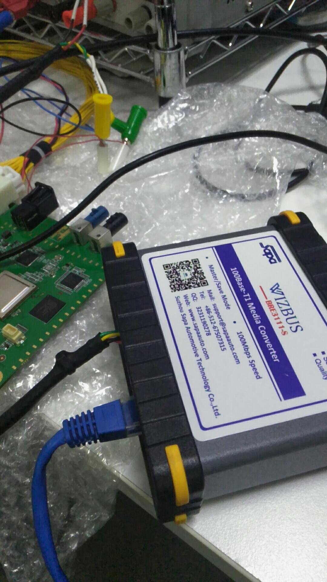
    And the link partner is as below,


    I will send you email about the driver code and schematic because I don't know how to upload documents in E2E.

    Thanks & Best Regards,

    Sherry

  • Hi Sherry,

    I'm glad to here the PHY can now link properly. Next, to verify the PING, can you put the PHY into a digital or analog loopback mode through register 0x0016

    0x0016 = 0x0008 //analog loopback

    0x0016 = 0x0004 //PCS loopback 

    And verify is data is able to transfer from the MAC over the RGMII interface of the PHY and back?

    Regards,
    Justin 

  • Hi Justin,

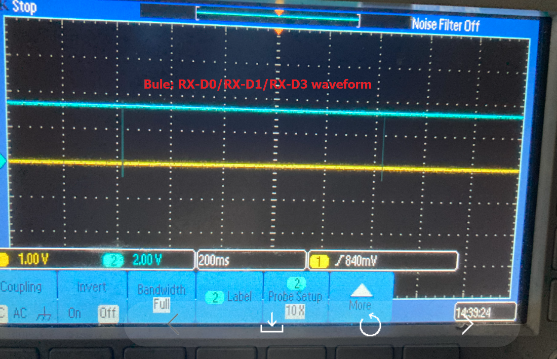
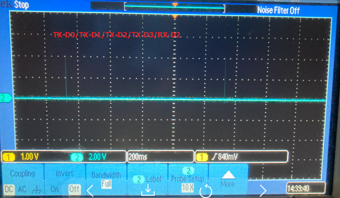
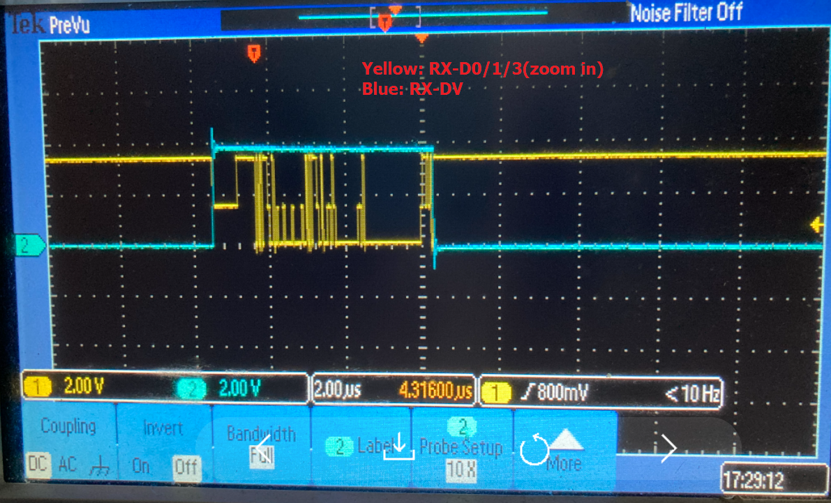
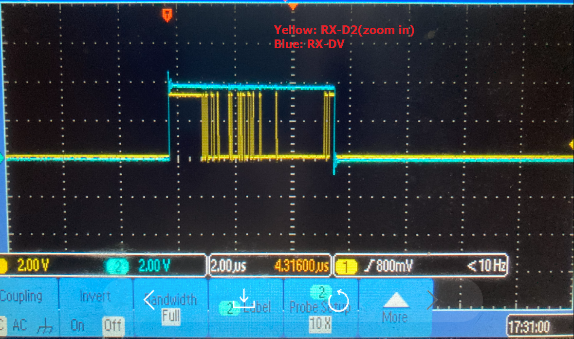
    The ping still can't work today. We test RX waveform as below, I also try to enable analog loopback and PCS loop back, and the waveform at RX is same. I also try to enable XMII loopback, but I can't enable it with unknown reason.

    RX-D0,RX-D1 and RX-D3 have the same waveform

    TX-D0,TX-D1,TX-D2 and TX-D3 have the same waveform as below. In addition, RX-D2 waveform is also as below which means that RX-D2 waveform is different form RX-D0/1/3, their polarity is opposite. I am not sure whether it is normal or abnormal. In the schematic, RX-D2 has a pull up resistor while RX-D0/1/3 not. I am not sure whether the pull up resistor impact RX-D2's polarity.

    We also test RX-DV, and it seems that our PHY receive valid data because RX-DV is high.

    For 0x00-1f, 467 register, I will send you email. I didn't see any error except 0x0017 register(0x17=0x424d). I use RGMII mode, so I can ignore bit0~5, right?

    Thanks & Best Regards,

    Sherry
  • Hi Sherry,

    In the register data provided, register 0x0016 shows that the PHY is not in a loopback mode. Can you ensure that you are able to properly configure the registers and see the result reflected? Can you also describe the SOC used oppostite the PHY on the RGMII interface?

    Regards,

    Justin 

  • Hi Justin,

    The register I sent to you is under the normal status instead of loopback mode. I did configure analog loopback and PCS loopback, but I just test the RX and TX waveforms which is same with normal mode, so I didn't dump the register under loopback mode. Could you please tell me RX waveform's polarity is normal?

    The SOC is TDA2E. The total link is TDA2E->811->100base-T1 link partner->PC. When TDA2E sent a Ping to PC, the PC can receive the data, and then PC send the data back to SOC, but SOC can't receive it. We don't know the failure is in the PHY or in the SOC, so we test the RX waveform. It seems that our PHY have data on RX pin and RX-DV is valid, but I don't know whether RX waveform is correct because the waveform's polarity is strange.

    I also check the strap register, and the register value matches with the value we set.

    Do we need to configure some registers when paired with SOC?

    Thanks & Best Regards,

    Sherry
  • Hi Sherry,

    I agree the waveforms on RX_D0/D1/D3 look incorrect. I expect the RX_D* pins to be low when data is not present and the intermediate voltage between the logic high and low is not expected. Can you confirm that there are no external pull-up/pull-down values on the RX pins between the MAC and PHY, and that the SOC is not driving the RX pins to create a contention between the PHY?

    I don't expect there are registers that are required when paired with a MAC or SOC to correctly configure the RX pins. Their polarity does not change, even with external strapping resistors. 

    Regards,
    Justin 

  • Hi Justin,

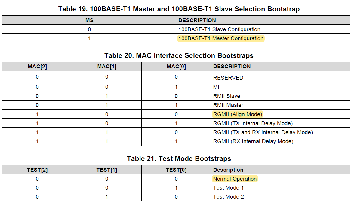
    The SOC feedback that they can detect the receive packet, but the packet is invalid, so the SOC didn't receive the packet. The SOC suspect 811's RX data is invalid(wrong polarity, wrong sequence or wrong mode configuration). Below is the customer's mode selection marked by yellow.

    1. When do we need to set master mode? When do we need to set slave mode?

    2. For the MAC interface selection, when do we need to set delay mode?

    3. There are no external pull-up/pull-down values on the RX pins between the MAC and PHY. And SOC feedback they don't drive RX pin.

    4. Do you have any other idea for this issue?

    In addition, what is the difference between the following four link status?

    Thanks & Best Regards,

    Sherry
  • Hi Sherry,

    1. Master and Slave modes are used to link two PHYs over the MDI interface. By being able to establish link, there does not appear to be an issue here.

    2. The RGMII delay mode is used to make sure the RGMII timing requirements in the datasheet can be met. Can you verify these timing requirements and provide the mode used in this application?

    3. Okay, Do all RX_D0, RX_D1, RX_D3 pins have the same waveform? There is also no internal pull-up or pull-down in the SOC, correct? Can you isolate these pins from the SOC and measure their waveforms in this scenario? 

    Regards,
    Justin 

  • Hi Justin,

    Good news, the ping works.

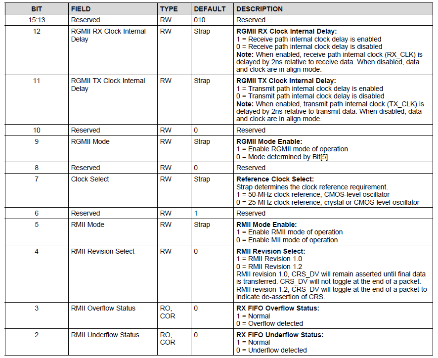
    The customer set 0x0017 bit[12]=1, then the ping works. But I don't understand why RX delay mode will solve this question. Is it related to the PCB layout?

    In addition, the RX waveform is correct. After ping works, I test the waveform again, it is same with before.

    Thanks & Best Regards,

    Sherry

  • Hi Sherry,

    Yes, the RX_CLK and RX data needs to be shifted in order to meet the required setup and hold time specification of the RGMII timing. This can be done in layout, registers, or a combination of both.

    Regards,
    Justin 

  • Hi Justin,

    In align mode, RX data and RX clock are sent out at the same time. In RX delay mode, RX data is first sent out, after 2ns, RX clock is sent out. In my understanding, align mode should work, but now only RX delay mode can work. There are also other customers encountering the same issue. Is there any other reason for this issue?

    Thanks & best Regards,

    Sherry

  • Hi Sherry,

    The RX data and RX clock need to be offset at the receiver, therefore a delay must be introduced between the signals. A delay can be handled in the layout of the signal traces, in which case, Align Mode can be used since the delay occur at the receiver side. If there is no delay in the signal routing, then Delay Mode can be used in the PHY to tune the delay to the necessary time to meet the RGMII timing specifications.

    Regards,
    Justin