This thread has been locked.

If you have a related question, please click the "Ask a related question" button in the top right corner. The newly created question will be automatically linked to this question.

ISO6740: How to avoid undetermined output

Part Number: ISO6740

Hi team,

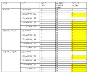
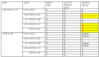
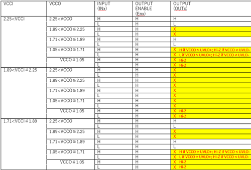
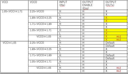
1. ISO67xxF output is undetermined when 1.89 V < VCCI, VCCO < 2.25 V and 1.05 V < VCCI, VCCO < 1.71 V.

My customer concerns that the case when VCCI or VCCIO ramp up or down slowly, the output can be undetermined.

Could you please advice how to avoid undetermined output?

Can you please let me know the reasonable ramp up or down rate to avoid undetermined output?


2. UVLO threshold is specified in the datasheet, but I don't find the detailed function from the datasheet.

Is it similar to powered down (PD) state described in datasheet 9.4?

Regards,

Itoh

  • Hello Itoh,

    Thank you for your questions. I've answered them in order below.

    1. The device takes 100 us to power up. So if the VCCI/VCCO ramp up can be less than 100us then the customer won't see any undetermined outputs.
    2. UVLO is the threshold which separates the powered up and powered down states of the device.  For supply voltages greater than UVLO+ the device is in powered up state, and for supply voltages less than UVLO- the device is in powered down state.

    Regards,
    Darrah

  • Hi Darrah-san,

    Thank you for the response.

    Can you please answer what's the case for ramp down as well?

    What is the recommended ramp down time to avioid undetermined output?

    Regards,

    Itoh 

  • Hello Itoh-san,

    For ramp down please try to keep the time close to 100us as well.

    Regards,
    Darrah

  • Hi Darrah-san,

    OK. Could you please elaborate on why <100us ramp down time works to avoid undetermined output?

    Regards,

    Itoh

  • Hi Itoh-san,

    We do not have a specification for ramp down time for the device. However, 100us is a short enough duration that the device will not be able to enter the undeterminable state. This is not a strict cutoff, and the customer can test with their system longer ramp down durations to find a time that works for their system and does not result in any undeterminable outputs.

    Regards,
    Darrah

  • Hi Itoh-san,

    Is the customer currently seeing issues with the device going into the undeterminable state during ramp down? Since we do not spec ramp down time, we unfortunately can not provide specific details of what to expect/how the device ramps down, but undeterminable outputs during ramp down is not a commonly seen issue.

    Regards,
    Darrah

  • Hi Darrah-san,

    Could you please elaborate on the exact definition of undetermined output?
    My customer doesn't understand how the output looks like when VCCO=PD.
    Is it mostly going to be floating as discussed in the thread below?

    https://e2e.ti.com/support/isolation-group/isolation/f/isolation-forum/968767/iso7760-device-functional-modes

    Also, if 1.89 V < VCCO < 2.25 V or 1.05 V < VCCO < 1.71 V, is the output going to be intermediate voltage (i.e. neither strong high or low)?

    Also just want to make sure, when EN=L an5 1.89 V < VCCI < 2.25 V or 1.05 V < VCCI < 1.71 V, is the output going to be Hi-Z?

    Regards,

    Itoh

  • Hi Itoh-san,

    When the device is powered down in the sense that VCCO = 0V or is very close to 0V, most of the outputs will be floating. This is because there is no power in any portion of the output circuitry of the device. As the power supply increases but remains within the voltage range below what is required to power up the device (range specified in the datasheet), the device will remain powered down but portions of the output circuitry may become partially powered. The partial power within the output circuitry can result in some intermediate voltages being seen at the output. This is why we refer to them as undeterminable, because during the ramp down/ramp up it is difficult to know exactly what portions of the device circuitry are properly powered and how that will impact the output voltages. Any voltage seen on the outputs during the undeterminable state would be weakly driven signals that are neither high or low.

    Yes, while EN=L, the outputs will be Hi-Z. When in high impedance mode, a pull up or pulldown resistor could be used to force a high or low.

    Regards,
    Darrah

  • Hi Darrah-san,

    Could you please if the table below correct?

    Also, my customer wonders why the output can be undetermined while INx = L.

    My customer assumes if the input signal is not modulated and transmitted through the isolation barrier when INx=L, the output should be stable.

    Looking at the datasheet Figure 9-2, it looks like the signal is modulated and passing through the isolation barrier when INx=L.

    Is this the case for ISO6740F version as well?

    Regards,

    Itoh 

  • Hello Itoh-san,

    In the table are the "X" used to indicate undeterminable? If this is the case then the table is mostly correct. I've made some changes below in red. When VCCO < 1.05 the VCCO can be considered powered down and the outputs will be Hi-Z. When VCCO is in the range 1.5 < VCCO < 1.71 and VCCI is in the operational range, the output will depend on the specific UVLO+ and UVLO- of the device. The UVLO+ and UVLO- will fall within the range 1.5V to 1.71V so the entire range will not have the same behavior.

    The undeterminable output is due to the VCCO side being only partially powered, so although the input signal may be received and transmitted across the barrier as expected, the output circuitry may not output the signal as expected. The two sides of the isolator operate independently so the state of the output signal is not impacted by the input state when VCCO is powered down.

    How the carrier signal behaves differs between the F and non-F versions of digital isolators. For F devices the carrier signal is "on" (transmitting a sinusoidal signal) when the input signal is high, and the carrier signal is "off" (not transmitting a sinusoidal signal) when the input signal is low. For non-F devices the carrier signal is "on" when the input signal is low, and the carrier signal is "off" when the input signal is high. So essentially when the input signal matches the default output of the device, the carrier signal will be off. If anything is not clear, please let me know.

    Regards,
    Darrah

  • Hi Darrah-san,

    Yes, X means undeterminable.

    I'd like to discuss a few points you added.
    First, you say if VCCO<=1.05V, the output will be high-Z.
    It is different from Table 9-2 in the datasheet (defined as undeterminable).
    Could you please elaborate on that?

    Also, I think if 1.05V<VCCO<=1.71V, you mentioned the output will be undeterminable which means intermediate voltage (neither strong H nor L).

    I think directly showing "H if VCCO>UVLO+; Hi-Z if VCCO<UVLO-" is a little bit confusing, so I think it should be better to keep it just "undeterminable".

    What do you think about it?

    I understand about the OOK part.

    Best regards,
    Itoh

  • Hi Itoh-san,

    The high-Z outputs occur when the output circuitry is entirely powered down. This occurs in the range from 0V up to potentially 1.05V. Table 9-2 in the datasheet is a more generalized or high level look of the device behavior. In reality the behavior of the device is slightly more complicated since thresholds will vary from part to part. For the most straightforward understanding of the device output, table 9-2 is correct.

    I agree that this distinction and the addition of UVLO+ and UVLO- can be confusing. For simplicity, leaving the table as it was originally would be okay. 

    Regards,
    Darrah