- Ask a related questionWhat is a related question?A related question is a question created from another question. When the related question is created, it will be automatically linked to the original question.
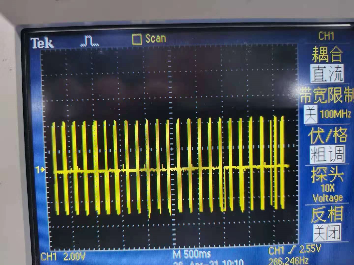
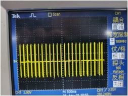
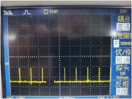
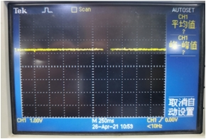
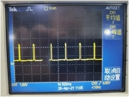
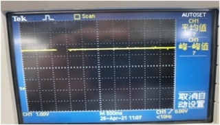
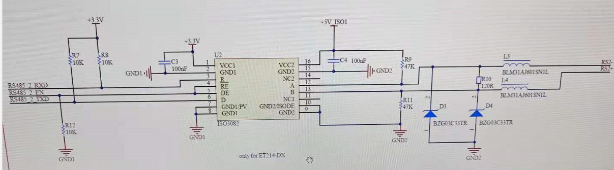
ISO3082 Abnormal communication waveform
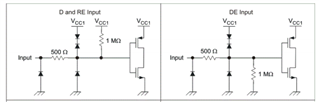
1. We have done the ABA cross test to confirm that the chip is defective.
2. MODBUS sends the same series of commands and receives different waveforms at the AB end.
The customer wants to know what causes the failure?
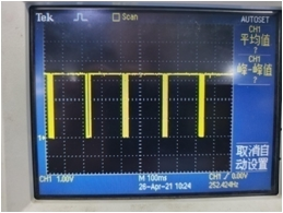
2.OK
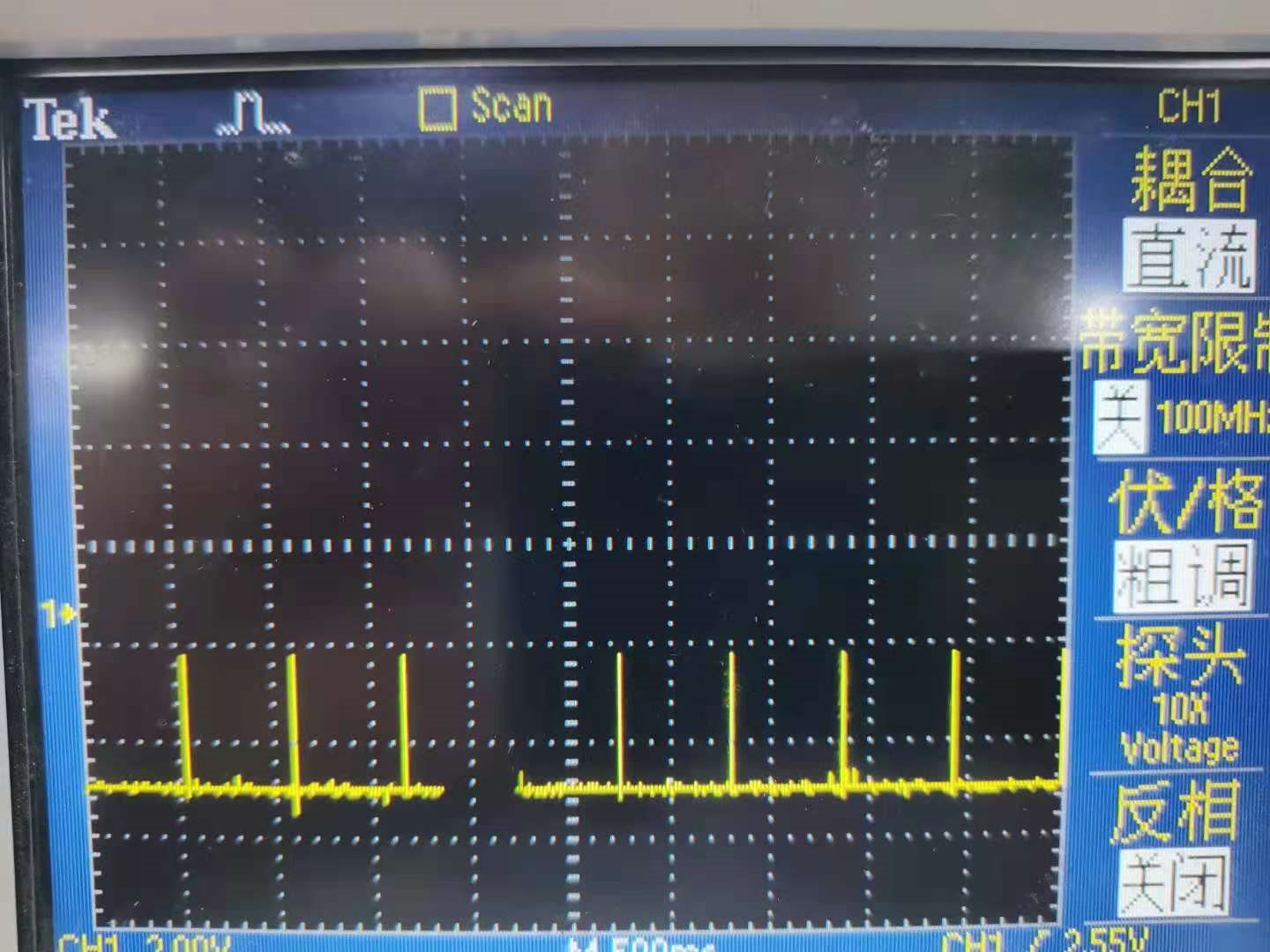
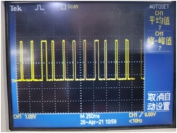
3.NG