This thread has been locked.

If you have a related question, please click the "Ask a related question" button in the top right corner. The newly created question will be automatically linked to this question.

ISO7741: SPI Data, the ADC data on the left side cannot be read

Part Number: ISO7741

Dears

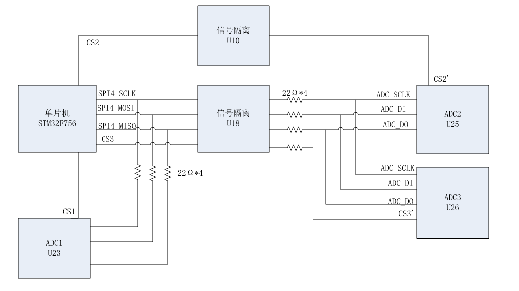
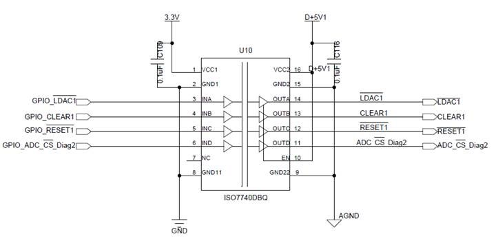
Iso7741 is used to isolate SPI data.
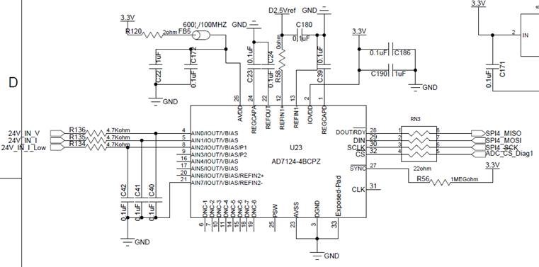
The left side of ISO7741 is a single-chip microcomputer and 1 ADC, and the right side of ISO7741 is 3 ADCs.
The single-chip microcomputer can only correctly read the data of the three ADCs on the right side, but the ADC data on the left side cannot be read. If iso7741 is removed, the ADC data on the left can be read correctly.

ADC-Analog Data Converter

Thanks

Elsa Duan

  • Hi Elsa:

    Thanks for posting your question on E2E.

    If multiple slaves share the same SPI bus, slave devices’ SDO should go high impedance when chip select is high.

    In your application, please make sure that the EN1 pin of ISO7741 is driven low when the left side ADC is being read. This puts the OUTD of ISO7741 into high impedance allowing the SDO of the left side ADC to drive the SPI bus correctly.

    Regards,

    Dushmantha 

  • Dear Dushmantha,

    Thanks for your advice.

    I connect the EN1 PIN to the IO port of the MCU for control according to your suggestion.
    Before pulling down the ADC1 chip select on the left side of ISO7741, first pull down EN1, pull EN1 high after reading ADC1, and then read ADC2 and ADC3 on the right side of the isolation chip.
    The result is the same as before. The result of reading the ADC1 status register is 0xFF, and the reading of Adc2 and Adc3 is normal.

    Can you help me? It's urgent.

    Thanks a lot.

    Elsa Duan

  • Hi Elsa:

    I'm sorry to hear that you're still having issues while reading the ADC1 status registers.

    Is it possible to share the schematic and SPI bus waveforms at the MCU while ADC1 status registers are being read? What is the SPI clock frequency in your application?

    We can reach out to you via email if you're unable to share the above information in this public forum. Please let us know your preference.

    Thanks,

    Dushmantha

  • Dear Dushmantha,

    Problem description: The microcontroller can read the data of ADC2 and ADC3 normally, but the collected data of ADC1 is 0 (the ready position of ADC1 is not 0).

    The principle block diagram is as follows.

    See the picture below for some schematic screenshots.

    Two methods have been tried:
    1. Solder U18 out. The data of ADC1 can be read normally.
    2. Solder the U18, and then short the U18 pad 3 and 14 with wires, 4 and 13 short, 5 and 12 short, 6 and 11 short. The data of ADC1, ADC2, and ADC3 can be read normally.

    Thanks

    Elsa Duan

  • Hi Elsa:

    Thanks for providing the system block diagram and the schematics.

    I don't see any issues with your approach except the U18 EN1 pin should be driven low when ADC1 SPI registers are being read.

    I understand that this is something you tried without any success.

    Can you please try tying EN1 of U18 to GND to see if you can recover the SPI communication from ADC1? This will eliminate the EN1 to CS1 timing requirements for debug purposes.

    To debug this issue further, can you please probe SPI4_SCLK, SPI4_MOSI, SPI4_MISO and CS3 waveforms while ADC1 status registers are being read? It would be useful to probe these SPI signals with (SPI communication not working) and without (SPI communication working) U18.

    Thanks,

    Dushmantha

  • Hi Elsa:

    Just checking in. Did you manage to make progress with this debug?

    Regards,

    Dushmantha

  • Hi Elsa:

    I'm closing this thread due to inactivity.

    Please feel free to click on yellow "Ask a related question" button on the top right hand corner of this page if you need any additional support.

    Regards,

    Dushmantha