This thread has been locked.

If you have a related question, please click the "Ask a related question" button in the top right corner. The newly created question will be automatically linked to this question.

SN74LVC3G14: Please review the schematic

Part Number: SN74LVC3G14
Other Parts Discussed in Thread: LMG1205, TLV3601, TLV3502, LMG1210

Hello TI experts,

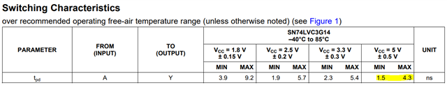
My customer considers to use SN74LVC3G14 and LMG1205 for their product, and I already got some advice for LMG1205 in previous post.

https://e2e.ti.com/support/power-management-group/power-management/f/power-management-forum/1103658/lmg1205-how-to-get-more-efficiency

and now I want you to review the rest of the schematic.

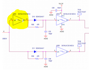
you can see 2 resistors, R89 and R99 below.

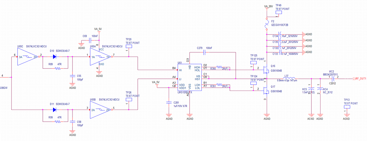
my customer already tested that reducing the value of R89 and 99, the efficiency got little higher. (it worked as they expected)

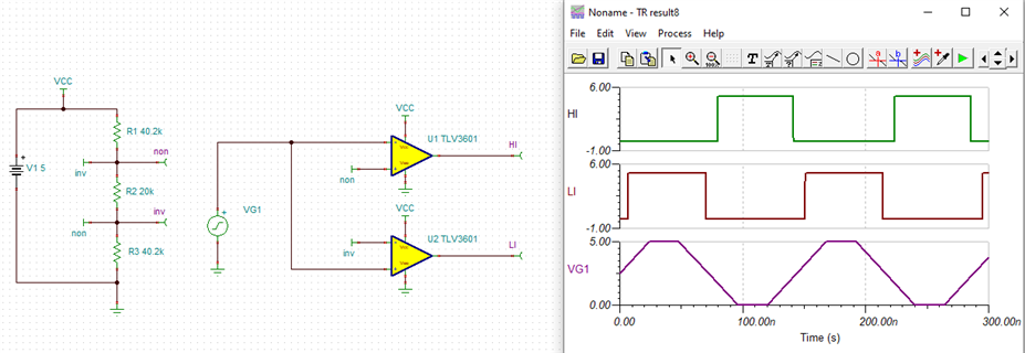
but as you know, if we reduce the value too much of R89 and R99, we may see the zero cross between 2 signals.

Do you have any idea about the minimum value of avoiding zero cross?

Please check this issue. Thanks.

Best regards,

Chase

  • Hi Chase,

    The circuit they are using is a falling edge delay circuit, which may be misleading since the delayed edge is going into an inverter -- so technically it's delaying the rising edge at the output.

    That means that they can control the rising edge of the HI signal and the rising edge of the LI input by varying R89 and R99, respectively.

    Assuming that zero overlap for the positive signals is permissible, then we need to look at the added delay from the inverter on the top circuit:

    We'd expect that delay to be between 1.5 and 4.3 ns:

    Given that info, we need to delay the bottom rising edge by at least that much to avoid overlap of the signals.

    Delay from an RC circuit into a Schmitt-trigger device can be precisely calculated due to the datasheet specs for thresholds using the RC charge equation:

    Vc(t) = Vcc * exp( -t/(R*C) )

    To get the delay, we need Vc(t) = V_T-, then solve for t... I'll just rearrange the equation first:

    t = -R*C * ln( Vc(t) / Vcc )

    Next I need to get the 5V values for V_T- from the datasheet. I use linear interpolation to get the exact value at 5V for both the min and max:

    min = 1.25V, max = 2.25V

    This let's me easily put it into excel and calculate your values of delay with R = 49 and C = 100pF:

    delay min = 3.9ns

    delay max = 6.8ns

    So it looks like we don't have enough delay here to guarantee that it won't overlap. We need to have at least 4.3ns for that. Just using the same equation and rearranging things a bit I can get the new resistor value required to guarantee that it won't have any overlap:

    R = -t/( C*ln(Vc(t) / Vcc)) = - 4.3n /(  ln( 2.25/5 ) = 53.85 ohms

    -

    I was going to start by saying that I wouldn't really recommend using a Schmitt-trigger logic gate for precision timing applications like this, but I figured it would be easier after explaining why. The threshold specs are just too wide.

    The only way to be certain that it will work would be to tune every board. An analog comparator + reference could eliminate that entirely by providing a much more consistent threshold.

  • Dear Emrys,

    Thank you for your support.

    I will discuss it with my customer, and send you results.

    and here is another question.

    The reason why my customer used schmitt-trigger inverter is all the reference is used schmitt-trigger inverter.

    (they used pSemi FET driver and now they check LMG1205. both reference are used schmitt-trigger inverter.)

    so, could you guide me about the combination of analog comparator and reference? (considering 7MHz signal frequency)

    A document, schematic would be fine. it will be a great help both my customer and me.

    Best regards,

    Chase

  • Hi Chase,

    I don't support comparators, but I've reassigned this thread to a team that does to see if they can provide assistance.

  • Hi Chase,

    I would encourage you to take a look at this app note about using one of our comparators to drive a GaN FET driver: https://www.ti.com/lit/an/snoaa82/snoaa82.pdf

    In the meantime, can you please answer the following questions?

    • What are your speed needs for the comparator? (Propagation delay)
    • What supplies do you have available?
    • How much hysteresis would you like to implement? (See https://www.ti.com/lit/pdf/SBOA313A for more info on hysteresis)
      • What are the thresholds that you need? VH/VL

    Best Regards,

    Joe

    Applications Engineer

    Linear Amplifiers Business Unit | Comparators Product Line (CMPS)

    All information in this correspondence and in any related correspondence is provided “as is” and “with all faults”, and is subject to TI’s Important Notice (http://www.ti.com/corp/docs/legal/important-notice.shtml)

  • Hi Chase,

    I actually believe that we can simplify your delay scheme if we use a dual channel, high speed comparator. 

    I would like to first confirm that you are trying to implement break before make (BBM) for the high side and low side FETs.

    Best Regards,

    Joe

    Applications Engineer

    Linear Amplifiers Business Unit | Comparators Product Line (CMPS)

    All information in this correspondence and in any related correspondence is provided “as is” and “with all faults”, and is subject to TI’s Important Notice (http://www.ti.com/corp/docs/legal/important-notice.shtml)

  • Dear Joe,

    Thank you for your support.

    Here are some answers which you asked.

    • What are your speed needs for the comparator? (Propagation delay) -> my customer uses 7MHz pulse signal. (high=5V, low=0V)
    • What supplies do you have available? -> my customer uses 4.2V battery power.
    • How much hysteresis would you like to implement? (See https://www.ti.com/lit/pdf/SBOA313A for more info on hysteresis) -> could you explain it more? i read the document bout there are many points that unclear.
    • What are the thresholds that you need? VH/VL -> could you explain it more?
    • you are trying to implement break before make (BBM) for the high side and low side FETs. -> Yes we are trying to implement BBM with very short time.

    If you need more information, please let me know.

    Best regards,

    Chase

  • Hi Chase,

    Thank you for providing that additional info. I will get back to tomorrow as today is a holiday. 

    Best Regards,

    Joe

    Applications Engineer

    Linear Amplifiers Business Unit | Comparators Product Line (CMPS)

    All information in this correspondence and in any related correspondence is provided “as is” and “with all faults”, and is subject to TI’s Important Notice (http://www.ti.com/corp/docs/legal/important-notice.shtml)

  • Hi Chase,

    I would like to provide a little more info on my ideas for how to implement break before make.

    Apologies for suggesting hysteresis earlier as I think we can create BBM without it.

    By configuring the comparator DC thresholds, we can create this overlap in the outputs where they are both logic low, meaning both FETs are never on at the same time. 

    As you can see by the simulation I am providing below, both HI and LI are ~40% duty cycle signals where the logic low of each overlap.

    I used (2X) TLV3601 high speed comparators with single-ended outputs that toggle between 0V and 5V.

    I would like to first confirm that the available supply for the comparator is 5V. With a 4.2V supply, the input signal cannot exceed 4.5V without violating the input common mode range of the comparators. Thus, I simulated with a 5V supply and 5V input signal. Let me know what you think.

    Please let me know if there is any way that you would like me to tweak the circuit further or if I missed anything. 

    Break Before Make.TSC

    Best Regards,

    Joe

    Applications Engineer

    Linear Amplifiers Business Unit | Comparators Product Line (CMPS)

    All information in this correspondence and in any related correspondence is provided “as is” and “with all faults”, and is subject to TI’s Important Notice (http://www.ti.com/corp/docs/legal/important-notice.shtml)

  • Dear Joe,

    Thank you for your kind support.

    first, they use boost converter to make 5V from 4.2V.

    and I have more questions, 

    1. Can I adjust duty cycle changing the ratio of R1, R2 and R3? what would be happen If I use 400K,200K,400K or 4K,2K,4K instead of original value?

    2. Is it a good choice that I use 5V voltage reference instead of boost converter output?

    (cause originally I heard that I can make same effect using analog comparator and voltage reference.)

    3. what is the important specification to choose comparator? Do I need anything other than toggle frequency and input voltage?

    Best regards,

    Chase

  • Hi Chase,

    Please see my feedback below:

    1. You can definitely change the resistor ratios for the DC references to the 100k ranges that you mentioned to keep the 40% duty cycle. You can also adjust the R2 value to adjust your break before make time. I would recommend maintaining a duty cycle of less than 45% to maintain BBM but you will have to adjust the resistor values to find what works best for your gate driver.
      1. What is your rise and fall time of your input signal?
    2. As long as you filter the boost output for the 3 resistor network, I do not see an issue with using the Boost output. You can use the boost converter output so long as the boost converter can source the two TLV3601 comparators (about 14mA) and the current draw of the resistor network which can be minimized by increasing the resistances as you suggested. 
    3. Some important specifications are the toggle frequency, input voltage range (input common mode range), minimum pulse detection, and propagation delay for high speed applications such as yours. Additionally, single-ended outputs (full supply swing) are important because gate drivers require such signals. This is why we suggest the TLV3601 for your application.

    Please let me know if you need any additional explanation or modification of the circuit I provided. I will reach out to you via friend request if you need further support.

    Best Regards,

    Joe

    Applications Engineer

    Linear Amplifiers Business Unit | Comparators Product Line (CMPS)

    All information in this correspondence and in any related correspondence is provided “as is” and “with all faults”, and is subject to TI’s Important Notice (http://www.ti.com/corp/docs/legal/important-notice.shtml)

  • Dear Joe,

    Thank you for your support.

    actually I think that my customer needs dual comparator, instead of 2 single comparators, because of the space of PCB.

    so I found TLV3502. it is suitable for my customer and fit to conditions what you mentioned.

    (we have to find IC which propagation delay is under 10ns, because we have to connect comparator with LMG1210. it has 10ns propagation delay.)

    Could you confirm that my choice is okay or not? and I would be very happy if you simulate with TINA using TLV3502, then my customer can test detailed things based on your simulation.

    Best regards,

    Chase

  • Hi Chase, 

    I just sent you a friend request so that I can support you further via chat. Please accept it at your earliest convenience. I will now close this thread.

    Best Regards,

    Joe

    Applications Engineer

    Linear Amplifiers Business Unit | Comparators Product Line (CMPS)

    All information in this correspondence and in any related correspondence is provided “as is” and “with all faults”, and is subject to TI’s Important Notice (http://www.ti.com/corp/docs/legal/important-notice.shtml)