Other Parts Discussed in Thread: SN74LVC162244A,
Hi,
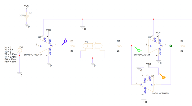
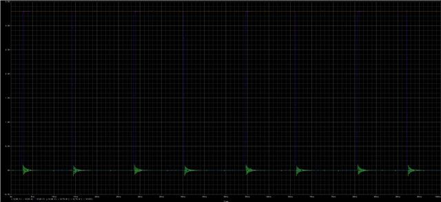
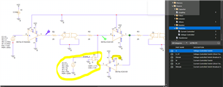
I designed a circuit with SN74LVC2G125 and SN74LVC162244A, which is shown in the first picture below. In my simulation results (shown in the second picture below), I am expecting the voltage at U1 pin 2 (green waveform) to be a delayed copy of the voltage at U2 pin 1 (blue waveform). However, what happens is that the voltage at U1 pin 2 is instead close to 0V, with some ringing as U2 tries to drive its voltage to U1.
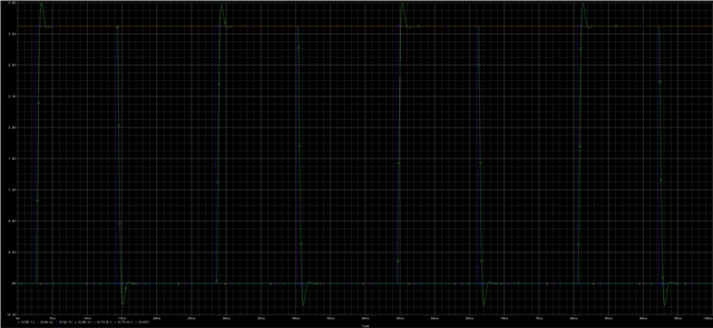
My hypothesis is that the output enable of U3 is not functioning properly, so as a result U3 is not in a high-impedance state and somehow interfering with the input of U1. The reason I suspect this is because when I connect U3's VCC to ground and re-run the simulation, I get the results shown in the third picture below, where the voltage at U1 pin 2 is now following the voltage at U2 pin 1 with some overshoot/undershoot and delay.
Now, my question is: why does it not suffice to raise the output enable of U3 to VCC to put it in a high-impedance state if the part number's datasheet gives such instructions? Why do we need to ground its VCC pin as well?
Thank you.