Other Parts Discussed in Thread: SN65HVD1781, , TPS62091, SN74LVC1G34, SN74LVC1G126
Hi.
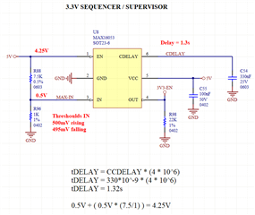
This circuit is designed to, when the 5V rail is turned on, 1.3s later the 3.3V rail is turned on.
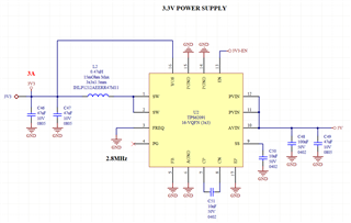
SN65HVD1781 is supplied on 5V rail, and at startup it will be set as receiver so there is the possibility of it to force 5V on the RO pin (receive out).
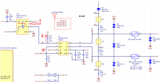
I have marked (1) and (2) in the third picture.
What can you say about these?
(A) About mark (1). While the 3.3V PSU with TPS62091 is still not running (before the 1.3s delay ends), if there is 5V on input A of SN74LVC1G125, then the 3V3 rail (VCC pin of it) would have 5V? Would it be better to place a resistor between RO of SN65HVD1781 and A of SN74LVC1G125?
(B) About mark (2). While the 3.3V PSU with TPS62091 is still not running (before the 1.3s delay ends), if there is 5V on RO of SN65HVD1781, then there will be a current flow from RO to the 3.3V rail through the 3.3K resistor (R23). I suppose that during this delay, because the EN pin of TPS62091 will be set low and TPS62091 supplied by 5V, and as I far as know when EN of it is 0, it places a load on its output to discharge the output capacitors.
(3) At 3.3V rail there are more 2x 47uF capacitors.
I have created 2 topics:
Question involving TPS62091, SN74LVC1G125 and SN65HVD1781 - TPS62091
Question involving TPS62091, SN74LVC1G125 and SN65HVD1781 - SN74LVC1G125
I think there is no need to create another topic for SN65HVD1781
Regards,
Jeferson