Other Parts Discussed in Thread: SN74AXC4T774, SN74AUC1G17, SN74AUC1G125-EP, SN74AXC8T245
Hello TI Experts,
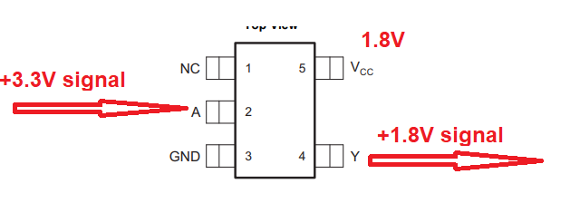
I am using TXU0101-Q1 to translate a 3.3V single-end signals to 1.8V, below is the schematic for your reference.
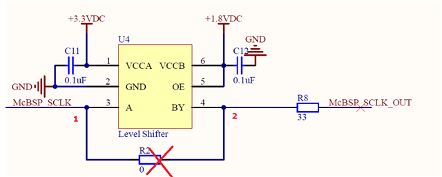
The McBSP_SCLK is a clock signal whose frequency is ~50MHz and duty cycle is 50%. I used the osc to measure the signals at postion 1 and position 2, respectively. Please see the below image. CH 1 is the signal @position 1, and CH2 is @position 2.
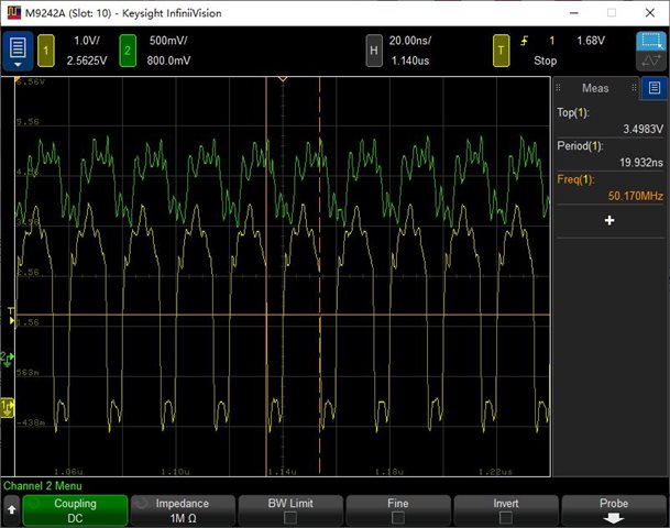
As you can see, the output of TXU0101-Q1 at position 2 is distorted if the freqency of the input is ~50MHz. It is always logical High. In the TXU0101-Q1 datasheet, the max data rate can be up to 200 Mbps when the device translates a signal from 3.3 V to 5.0 V. I am wondering the performance of this chip does not meet the requirement in my application, because when I reduced the frequency to ~10MHz, my system worked well.
Questions:
- The data rate in my application is ~50Mbps? What is the definition of the data rate and how to calcuate it?
- I reviewed the FAQ, do I have to choose another level shifter with higher data rate, like SN74AXC4T774 (310Mbps)?
Thanks.