This thread has been locked.

If you have a related question, please click the "Ask a related question" button in the top right corner. The newly created question will be automatically linked to this question.

SN74LXC1T45-Q1: Electrical Characteristics Table

Part Number: SN74LXC1T45-Q1

Hi,

Can you explain what this table means from the datasheet?

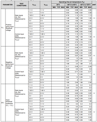
My understanding is that for the DIR pin, VT+ gives the voltage range of a logic high (A to B) and VT- gives the voltage range of a logic low (B to A). But what does this table mean for the data pins? Do these pins have logic high and logic low levels as well?

Best,

Lucas

  • All digital input pins have two states, high or low.

    This table describes the switching thresholds; it does not care about the meaning of the pins. For the data pins, their state determines whether the corresponding output pin drives high or low.

  • Hi Clemens,

    Does this mean this device doesn't translate the exact voltage level on pin A with respect to VCCA? For example, if VCCA = 3V, A = 1.5V, and VCCB = 5V, does this mean the voltage on pin B will be 5V or 2.5V? If A = 1V, will pin B be 0V or 1.6V?

    What if the voltage on pin A is outside of the ranges specified for logic high and logic low? Is this undefined behavior?

    Best,

    Lucas

  • This is a digital device.

    When the input voltage is between VT− and VT+, you do not know whether the output is high or low.

    To amplify analog signals, use an opamp.