Other Parts Discussed in Thread: ADS1298, TXB0104, TXB0106
Hi
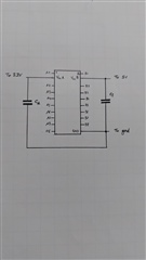
I use a TXS0108E for interfacing an Arduino Leonardo (works in 5V) and a sub-board featuring two ADS1298 ADC (work in 3.3V). The TXS is mounted on a HVV-221 adafruit-like board that has two capacitors between the 5V (resp, 3.3V) rail and the ground. It is used to shift the voltage on the SPI bus, chip selectors and other stuffs.
A simplified schematics is joined, note the transistor used to make sure that the HIGH level on the Output Enable pin is 3.3V and not 5V. (It is hastly drawn, my apologies)
Up until Friday, it used to work like a charm and I could properly pilot the ADCs and retrieve 500 samples per seconds of data from them.
This weekend, I let the whole system powered on (the PSU also powers ancillary systems that need some time to stabilise) and when I resumed data aquisition on Monday morning, the Arduino only sent 0xFF's to the computer.
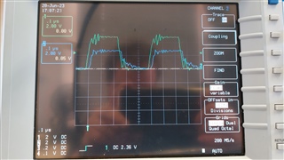
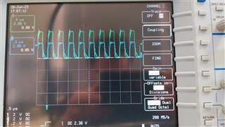
I unplugged the sub-board, pulled down the MISO to the ground via a 8.2k resistor and proceeded to record signals on the SPI bus via a Saleae Logic Pro 16 signal tracker and this is what I've got :
In each case I'm trying to read the identification of the ADS1298 : I'm sending three bytes (read registers starting from REG_ID ; read 1 + 0 register ; then a 0x00 and the answer should be sent on the same time.)
On the first picture, the level-shifter is also unplugged from the Arduino and the signal is directly taken from the Arduino pins. You can see 3 * 8 clock clicks on the SCK as expected, on the MOSI : 0x20; 0x00; 0x00, and on the MISO, only 0's as nothing is plugged in. So everything is normal.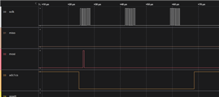
Now if I plug in the level-shifter board and take the signals on the 5V side, here is what I've got : the MISO follows the SCK, which explains the 0xFF's that I recorded earlier this morning.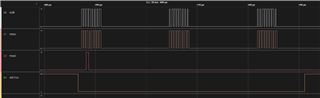
Finally if I take the signals from the 3.3V side, this is what is recorded : only one pulse out of eight on the clock and two pulses on the MISO.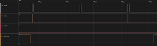
I don't understand what happens. Could it be that the TXS0108E be damaged from being powered on for almost 3 days ? I welcome any lead to help me restore last week's state !
Thanks in advance !