This thread has been locked.

If you have a related question, please click the "Ask a related question" button in the top right corner. The newly created question will be automatically linked to this question.

LSF0108-Q1: Thermal analysis for LSF0108-Q1

Part Number: LSF0108-Q1
Other Parts Discussed in Thread: LSF0108

Hi Team,

Could you please kindly help to check for LSF0108-Q1 maximum power could be calculated follow by below formula. VCCA=3.3V,VCCB=1.8V. From datasheet shows channel maximum Io=128mA, based on customer requirement they would open 6 channel at the same time. So Pmax=(3.3V-1.8V)*0.128*6=1.152W? 

Based on above calculation, customer has some concern for thermal rising, from datasheet it shows the thermal resistor is 74.3W/℃ , and customer ambient temperature would reach to 85℃, so seems the junction temperature may above 150℃.

Question as below:

#1 If the Pmax evaluation is correct?

#2 If we have thermal resistance based on our EVM evaluation result which could provide to customer for reference? Customer PCB board has 8 layer, maybe the thermal resistance would smaller, but we don't have some reference value which could provide to customer for their theory analysis. 

Thanks a lot for your support.

Best regards

Jie 

  • This is not how the LSF works.

    When the input voltage is below 1.8 V, the LSF behaves like an analog switch, and the A and B pins are connected directly, with about 9 Ω. When the input voltage is above 1.8 V, the switch is open, and the voltages are determined by the pull-up resistors.

    So for low signals, the power dissipation inside the chip is 6 × 9 Ω × I², where I is the actual current through the switch. (That current is VCC / Rpullup (with VCC and Rpullup from the output side).)

  • Hi Clemens

    Thanks a lot for your feedback.

    For your reply, could you possible help to clarify for the power dissipation calculate? 

    #1 With input voltage below 1.8V, then the power dissipation is 6*9ohm* I², I=VCC/Rpullup, since customer supply is 3.3V and 1.8V, So, under this kind of condition, which voltage refer to for the VCC in this formula ? Also for customer work voltage is above 1.8V, so this calculation is not suitable for customer application correct?

    #2 With input voltage above 1.8V, then how to calculate the power dissipation? 

    Thanks again for your support help to double check.

    Best regards

    Jie

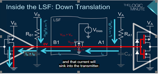
  • 1. When the device on side A pulls the signal down to 0 V (i.e., A is input and B is output), then the A and B sides are connected through the switch, and that device sinks the current that flows through both pull-up resistors. The current through the VCCA pull-up does not flow through the switch, but the current through the VCCB pull-up does.

    2. When the voltage is above Vref_A, the switch is open, and no current flows through it.

  • Hi Ladisch,

    So, from my understanding based on your description, for application with 3.3V to 1.8V level shift the power dissipation almost equal to 0? Since the internal switch is open? Could you please kindly help to clarify further for this?

    One more question comes from customer is how could they select the pull up resistor RB and RA. For customer application, the VA=3.3V and IO current limitation is ±5mA, for VB=1.8V and IO current limitation is 4mA, below is a customer estimate block diagram for the current flow, for example if VA is output and VB is input, then the current input to the VB port is IA+IB, is that correct? If not, could you also possible help to clarify it? Thanks again for your support.

    Best regards

    Jie

  • When the signal is high, the current is zero. When the signal is low, current flows through the switch. (In the latter case, the power dissipation is very small.)

    The diagram is correct.

  • Hi Clemens,

    (1) As you said,  for example VerfB=3.3V, VerfA=1.8V, B1 is the enable PIN , which conducts from B1 to A1; When B1 is high, the current passing through LSF0108 is 0; When B1 is low, The current passing through LSF0108 is VerfB/RpullupB =3.3V/1kohm=3.3ma, while the current passing through B1 side IC  is VerfB/RpullupB+VerfA/RpullupA=3.3V/1Kohm+1.8V/1Kohm=4.8mA;  Is it right?

    When the signal is high, the current is zero. When the signal is low, current flows through the switch. (In the latter case, the power dissipation is very small.)

    The diagram is correct.

    (2)  If we use all 8 channels,  when input side (A or B)voltage is low,  the worse case power consumption is 8× 9 Ω × (3.3V/1kohm)^2=784.08 mw. From datasheet it shows the thermal resistor is 74.3W/℃ , and our ambient temperature would reach to 85℃, so seems the junction temperature may above143.25℃.  Is it right? The power dissipation is high. So we should use larger than Rpullup,which value is 1kohm. 

    In short we are mainly concerned with the selection of pull-up resistors on the A and B sides  of LSF0108-Q1. Please give us  clear reference values of pull-up resistors , rather than some vague design suggestions.

    One more question comes from customer is how could they select the pull up resistor RB and RA. For customer application, the VA=3.3V and IO current limitation is ±5mA, for VB=1.8V and IO current limitation is 4mA, below is a customer estimate block diagram for the current flow, for example if VA is output and VB is input, then the current input to the VB port is IA+IB, is that correct? If not, could you also possible help to clarify it? Thanks again for your support.

    When the signal is high, the current is zero. When the signal is low, current flows through the switch. (In the latter case, the power dissipation is very small.)

    The diagram is correct.

    This is not how the LSF works.

    When the input voltage is below 1.8 V, the LSF behaves like an analog switch, and the A and B pins are connected directly, with about 9 Ω. When the input voltage is above 1.8 V, the switch is open, and the voltages are determined by the pull-up resistors.

    So for low signals, the power dissipation inside the chip is 6 × 9 Ω × I², where I is the actual current through the switch. (That current is VCC / Rpullup (with VCC and Rpullup from the output side).)

    Best regards,

    Bright

  • 1. Correct.

    2. What pull-up values to use depends on the speed you want to achieve, and the capacitance of the board. (The speed of rising edges on the B side is limited by the low-pass filter formed by the resitors and the capacitance.) For I²C, the total pull-up current is limited to 3 mA. What protocol are you using? What are the trace lengths?