This thread has been locked.

If you have a related question, please click the "Ask a related question" button in the top right corner. The newly created question will be automatically linked to this question.

LSF0108-Q1: Pull up resistors and capacitive coupling Ax <-> Bx

Part Number: LSF0108-Q1
Other Parts Discussed in Thread: LSF0108

Dear experts,

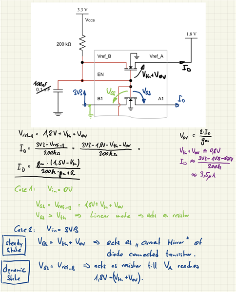
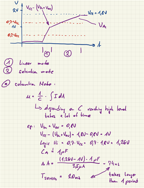
we are using LSF0108-Q1 as levelshifter between 3V3 (uP) and 1V8 (WiFi IC). CLK frequency is about 50MHz.
In our design (at the moment) 47k pull up resistors are used. Signal speed ist 50MHz.  In my opinion this should not be working / is not a robust design.
But in lab we see operation and I'm wondering why we have on A side a logic signal.

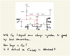
An idea is, that capacitive coupling between port B and A is high and we have some charge injection.
So i wanted to ask, is this the capacitance from B to A when B side (higher voltage) has a logical high and cascode transistor of LSF0108 is turend off?

Thanks,

Martin

  • For voltages below Vref_A, the LSF acts as an analog switch, so when using the B side as input and the A side as output, the pull-up resistors do not have much of an effect. (In some cases, the pull-ups on the A side could be omitted.)

    The pull-up transistors affect the output signal when translating up.

  • Hey Martin,

    When a logic HIGH is propagated through the device, the internal FET goes into an open state and I/Os rise to their respected voltages. There will be no current floating through the channels. Also see The Logic Minute Video Series for more information.

    Regards,

    Jack 

  • This is my understanding of this levelshifter


    Is therean error in my understanding?

  • Hey Martin,

    The LSF device only operates in cutoff region and the triode region during normal operation. During the cutoff mode, a logic HIGH is being transmitted into the output. Note that the internal FET becomes high-impedance during this state, where the I/Os are isolated and are being pulled up to their respective voltages by external pullups.

    Cds is not explicitly quantified in the datasheet, but note that Cio is the capacitance of the I/O terminal when the input conditions establish a high-Z state at the output. 

    Regards,

    Jack