Part Number: CD74HC4050
Other Parts Discussed in Thread: SN74ACT08
Hi expert,
Customer has some failure and I want to get the internal structure of CD74HC4050M96 for better explanation.
BR
Emma
This thread has been locked.
If you have a related question, please click the "Ask a related question" button in the top right corner. The newly created question will be automatically linked to this question.
Part Number: CD74HC4050
Other Parts Discussed in Thread: SN74ACT08
Hi expert,
Customer has some failure and I want to get the internal structure of CD74HC4050M96 for better explanation.
BR
Emma
Hi Emma,
Could you give some details as to what the failure is? If you provide some scope shots of what's going wrong, a schematic of how the customer has configured the device, a detailed description of the issue, etc. then I would be more than happy to try and assist you with the problem.
The internal design of the device is proprietary information which we can't really provide to you.
Best,
Malcolm
Hi Malcolm,
They will have this kind of phenomenon.
The input is 3.3V, but the output could be 1V or 0.36V.
and since the project will go mass production soon.
they need TI to analyze the potential reason quickly.
I read this article ,https://www.ti.com/lit/an/szza036c/szza036c.pdf
And I only find the Technology :HC/HCT – High-Speed CMOS Logic
I don't see this device has any special features, could you kindly help to confirm that?
C – Configurable VCC (LVCC) D – Level-Shifting Diode (CBTD) H – Bus Hold (ALVCH) K – Undershoot-Protection Circuitry (CBTK) R – Damping Resistor on Inputs/Outputs (LVCR) S – Schottky Clamping Diode (CBTS) Z – Power-Up 3-State (LVCZ)
their SCH is as below. if their MCU has a long trace to the input of the buffer, is there any risk?
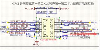
This device is really old, do we have a P2P device with better performance?
BR
Emma
Hi Emma,
There aren't any of those special features with this device. Long traces to the input also run the risk of reflections if you don't match impedances which could definitely affect device performance. It's harder for me to debug without seeing scope shots of the input/output/power. Nothing looks inherently wrong with your connections.
There are no exact P2P devices that will perform better. I'd recommend the SN74HCS365DR but this device is not P2P. It's also 3-state outputs instead of push-pull.
Best,
Malcolm
Malcolm,
What is the output current for recommendation?
We can only see the max current is 25mA on datasheet, but I can see another drive current on another slides.

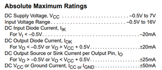
I don't know how to understand it. Since customer can measure the output current peak value is 8mA, RMS is about 2mA.
and customer also replace the CD74HC4050M96 with SN74ACT08(with another input always high) on the same board.
they try many times and the fail will not happen again, so I want to check whether it is the output drive current cause the issue.
BR
Emma
The colored table shows recommended output currents. This is the largest output current for which a voltage drop is specified and guaranteed. Exceeding this current is allowed (up to the absolute maximum rating), but then the output voltage is no longer guaranteed.
The recommended output current can be found as a test condition for the VOL/VOH specifications. It depends on the supply voltage, so for HC at 3.3 V, it will be less than 4 mA.
If this problem happened only once, then I'd guess that that chip got damaged, probably due to overvoltage (ESD).
Clemens,
Thanks for your answer on the output current explanation.
Besides, in this video: www.ti.com/.../basics-of-logic-and-translation.html. it shows output current for gates and drivers.
Could you kindly give me more explanation on it?
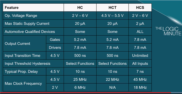
for the failure, which the output can not track input. Unfortunately, it happened on many machines.
their output is drive a transistor and the schematic is as below:
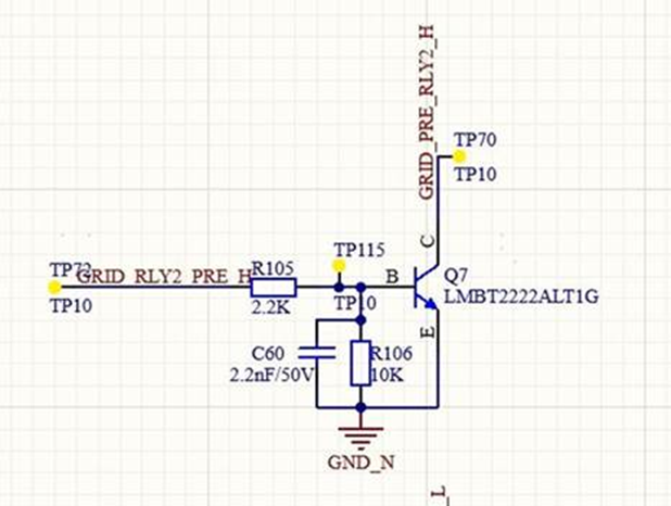
the output trace is quite long(since the transistor is one the other board), but it is not a high speed signal, it is only for on and off to drive next stage relay.
and the R105 in the schematic is close to the transistor.
Still, the oscilloscope can measure -3.6V voltage on output pin when the relay is turn-on. (still not very clear it is a noise into oscilloscope or the buffer device pin is also affected.)
so if there did some noise can affect the output pin, do you have some recommend method to improve it.
BR
Emma
Hi Emma,
Did you mean 0.36V like you said earlier?
Have you tested the part in isolation from this transistor? I would really like to see if the part works as expected in isolation from this second stage.
The picture you posted is again just stating what the recommended output currents are. You can exceed these but, as Clemens said, the output voltage is no longer guaranteed once you do. In other words, if the output is giving 8mA of current like you mentioned the output voltage might not be as expected for HC devices, although I wouldn't expect it to be that much of a difference.
Best,
Malcolm
Hi Malcolm,
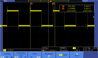
I just get some damaged part from customer and do bench test, with a 3.3Kohm as output load.
VCC=5V,
Input 100khz square waveform,high level =4.7V Low level =0.1V.
The good device output voltage level is correct:
However, the damaged part output voltage level is incorrect:
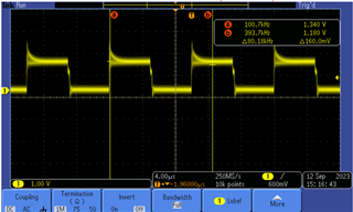
I have test two channels and both channels are abnormal, so what could be the potential reason to cause the damage?
Could the internal voltage supply circuit is wrong?
BR
Emma
Hi Emma,
There are a few possibilities:
Otherwise, if you don't think any of these things are issues, there's nothing more I can see that might explain why the part isn't working. It is an old part on an old die.
Best,
Malcolm
Malcolm,
Thanks for your explanation.
In my test, I just use the signal generator and input transition time is very fast.
and what is the requirement for the transition time? Is this requirement? Then it must be followed.

Besides, I can not find the ESD level for this part, CD74HC4050M96. Could you kindly give me more information?
BR
Emma
Malcolm,
Besides, they reported the failure after the machine running some time, so they don't think it is caused by ESD.
And they capture some spike voltage on output pin, do you think it will break the device? the duration is less than 10ns.
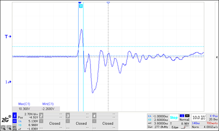
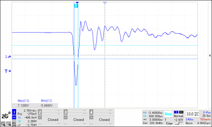
Since there is no description on output pin voltage on absolute value, so I just want to check it with you.
Another confusion is, on the same device, different channel, they can see similar voltage level waveform, you mentioned the phenomenon is ESD damage, so do you think all the ESD circuit are damaged at the same degree?
BR
Emma
Since we are now discussing this issue offline I'm going to go ahead and close this thread.
Best,
Malcolm