- Ask a related questionWhat is a related question?A related question is a question created from another question. When the related question is created, it will be automatically linked to the original question.
This thread has been locked.
If you have a related question, please click the "Ask a related question" button in the top right corner. The newly created question will be automatically linked to this question.
Dear Team,
Could you help to double check the schematic as below?

Many Thanks,
Jimmy
LVC devices are not guaranteed to accept 3.3 V signals with a 5 V supply.
Use a translator like the TXU0102.
Hi Ladisch,
Thanks for your reply.
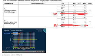
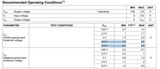
Is it because thedatasheet does not write the voltage range of VT+ and VT- when VCC is 5V, so it cannot guarantee that it can receive 3.3 V signals? Can you help me test the voltage range of VT+ and VT- at 5V? grateful
The rise time requirements of the two signals VGA_HSYN and VGA_VSYN are very strict, and LSF0102 cannot meet the requirements; according to the LSF series product calculation formula on TI's official website, Trise=2RC=2X4.7KX15pF=141ns, which is much larger than the 5.36ns required for the VGA_HSYN and VGA_VSYN signals.

1. The datasheet shows the Vin range is 0~5.5V, and the Vout range is 0~VCC; my current usage scenario is that when the 3.3V signal level is input, VCC=5V, and the output is VCC=5V, it should be OK, right?
2. When VCC=5V and the input is a 3.3V signal, only VT+MIN<3.3V and VT-MAX<3.3V should ensure normal reception of the 3.3V signal input, right?
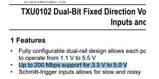
3. The data sheet of the TXU0102 you recommend also has a rate limit of less than 200Mbps. If there is a rate limit, there should also be a Trise limit on the output, right?


Many Thanks,
Jimmy
Hi Jimmy,
You can refer to the FAQ here for values that are not shown on the datasheet: What method is best used for estimating specification values between those given in the datasheet?
If you are looking to change to a TXU or LSF device, I would recommend you to make a new post on the translators forum.