This thread has been locked.

If you have a related question, please click the "Ask a related question" button in the top right corner. The newly created question will be automatically linked to this question.

SN74ALVC164245: Input and Output Not Matching in Some Instances

Part Number: SN74ALVC164245

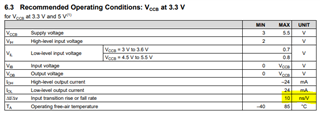
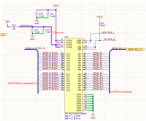
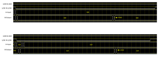
In my design, SN74ALVC164245 is used to translate 3.3V 16-bit data to 5V 16-bit data. The component works fine for the most part but there are instances where the input doesn't match the output for some bits. Some of the examples are shown below. Is there an explanation for this? How can this be solved? 

Thank you

  • Hi Simran,

    Typically, if observing an unknown output, this would mean the LVC device (VCC) is powered on with some of the inputs floating (i.e an unknown input for an unknown output).

    The recommendation is to ensure all the inputs of the LVC devices are at known states (high or low), as I suspect this is not the case for the instances of concern.

    If not, please help further clarify, thanks.

    Best Regards,

    Michael.

  • Hi michael, the inputs are at known state for the instances of concern. Whenever these instances occur, the outputs are high when they were supposed to be low. I donot have pull up in the inputs. 

    Regards,

    Simran

  • Hi Sirman,

    Could you help clarify the state of the input when you say the outputs are high instead of low?

    Also, any gaps with section 10 of the datasheet?

    Best Regards,

    Michael.

  • The design follows section 10 of the datasheet. From our test (see below), the OE is enabled for 256ns and we see that the input stays constant (eg 1. D1D0). However, the output is the same as the input (D1D0) for about 212ns, but changes to FFDO for about 4ns and goes back to D1D0. Is there an explanation for that glitch in the output even though the input hasn't changed? 

    Regards,

    Simran 

  • Hi Simran,

    There could be a few reasons, are there any glitches with the supply as well?

    Did the glitching re-occur? Or mainly after powering up? Could you also confirm OE is enabled after inputs are already toggling? Do you still see glitches when OE is enabled before the I/Os?

    Best Regards,

    Michael.

  • There is no glitch with the supply.  The supply is 3.3V on the VCCA and 5V on VCCB. The glitching occurs every 2-3 minutes. 1OE and 2OE in the figure are the enable signals for the chip and there is no glitch on that signal. OE is enabled around the same time the inputs are confirmed. In the test, the OE is enabled for 256ns. Once the input is set to the certain value, it doesn't change for the duration the OE is enabled. The output is the input value for certain time, then there is a glitch for 4ns and goes back to the input value after that.  

  • Also, does this chip require a strict power up sequence? Does VCCA need to be supplied before VCCB? What happens if this sequence is not followed? 

  • Hi Sirman,

    Thanks for clarifying. 

    It is interesting that the glitch is not occurring during power up as the below is for what could happen if any gaps in the power sequence recommnedation (mainly during power up, and back to normal once fully powered / ramped up).

    However, the provided waveforms do not tell much (input's transition rate, voltage levels of the I/O etc).

    Could you also help confirm the I/Os are actually switching at 3.3V and 5V while the inputs are not slower than the below? Is the glitch consistent with all outputs or just one? If so, do you still observe the glitch with no load (everything disconnected) at the outputs?

    Best Regards,

    Michael.

  • Could you confirm about the power up sequence? The datasheet mentions "proper power-up sequence". Does this mean VCCA has to be supplied before VCCB? What happens if this sequence is not followed?

  • Also, we have two 0.1uF bypass capacitors for VCCA and two 0.1uF bypass capacitor for VCCB. Is that enough or do you recommend a higher value? 

  • Hi Simran,

    Does this mean VCCA has to be supplied before VCCB? What happens if this sequence is not followed?

    Yes, VCCA is the supply that controls the device. Hence, recommended to be ramped up first so that the internal circuitry is all active and there's no internal floating node. Glitches during power up, as well as the concerns highlighted in section 10 can occur if the recommended sequence is not followed.

    Also, we have two 0.1uF bypass capacitors for VCCA and two 0.1uF bypass capacitor for VCCB. Is that enough or do you recommend a higher value? 

    It all depends on the system's power supply used i.e one 0.1uF is typically enough. However, if the power supply is still noisy, more/higher would suffice, thanks.

    Best Regards,

    Michael.