This thread has been locked.

If you have a related question, please click the "Ask a related question" button in the top right corner. The newly created question will be automatically linked to this question.

TXB0104-Q1: TXB0104-Q1 one-shot doesn't work during power-up

Part Number: TXB0104-Q1
Other Parts Discussed in Thread: TXB0104, TXU0304-Q1, TIDA-00296

Hi BU team 

My customer reported txb0104-Q1 didn't always output any waveform after powered-up. 

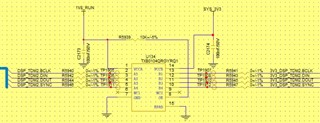
The schematic is shown in below screenshot. The DSP send 12.28MHz BCLK signal from I2S interface with 3.3V voltage to TXB0104 then output 1.8V voltage BCLK signal. The BCLK trace would directly drive two SOCs (1 to 2 channel).

There are two power-up sequencing. 

1. After VCCB and VCCA are stably supplied to TXB0104, DSP send the BCLK signals to TXB0104 then TXB0104 always work normally.


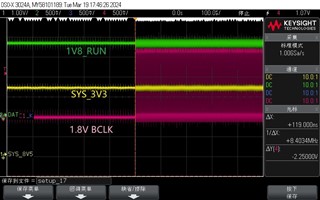
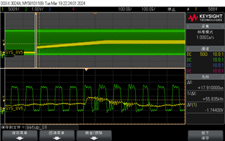
2. VCCB(3.3V)  is firstly supplied and BCLK from DSP also  is feed into TXB0104 simultaneously,then VCCA is supplied to TXB0104 and there is about 700us soft-start for VCCA power regulator which is shown.

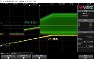
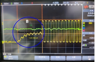
Under this power-up sequencing, TXB0104 has low possibility of no expected 1.8V BCLK output. The abnormal waveforms can be found in below screenshots.

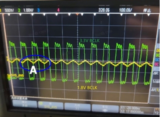
Customer also do another try under power-up sequencing 2. Create an OE delay via adding a capacitor to GND which is in parallel with R5939. Thus TXB0104 will be enabled after VCCB and VCCA are powered. During the t_EN duration,  the waveform marked B show the similar behavior with waveform marked A where txb0104 does work abnormally.  Customer thought that one-shot didn't work then result in no 1.8V BCLK output during power-up sequencing 2.  

Would you help share your comments? What's the solution under power-up sequencing 2?

Thanks 

  • I have no definite explanation why the device behaves the same as if OE were not high.

    But you have four unidirectional signals. A unidirectional translator like the TXU0304-Q1 would be much simpler and more robust.

  • HI Clemens

    Now this project will be SOPed at April and no chance to re-design TXU0304-Q1.

    For this project is urgent, would you help double check with designer and align it inside BU team and provide the supports?

    Thanks very much. 

  • I am not a TI employee; I cannot explain why a slow supply ramp would not enable the one-shots.

  • Hi Ted,

    Please help note the below datasheet recommendation. Hence, solution as ensuring OE is delayed enough for both supplies fully ramped up.

    However, not delayed long enough to violate the datasheet's input transition limit, thanks.

    Best Regards,

    Michael.

  • Hi Michael

    Thanks for your comments.

    But customer has below further questions and application concerns to be got supports. 

    1. In the AN A Guide to Voltage Translation With TXB-Type Translators,  it is also ok that the OE pin is tied to the VCCA via a 10kohm resistor when no specific output level in customer's application. and TIDA-00296 ref. design also adopt this connections.  So customer don't think that ensuring OE is delayed enough for both supplies fully ramped up. Pls double check it and share your comments. 

      If it is ok, when will the input signals are sent to TXB0104-Q1? Before  and after the VCCA(OE)/VCCB is fully ramped up in the schematic ? pls share your comments and the risk when doesn't meet this requirements. 

    2. But I can't understand your comment on violating the input transition limit listed in datasheet.  Can you share more comments what causes input transition too faster than recommended ?

    3. When issue happed in customer case, is it resulted in by the one-shots always working in off-state or the slow OE ramp up caused by the VCCA's supply soft-start  in customer design?  

        What's the requirement on OE ramp-up ? Doesn't get it in the datasheet and published application notes. 

    Thanks 

  • Hi Ted,

    1. Using just a pull-up without capacitor on OE do not act as a delay circuitry. Please confirm your delay circuitry is not violating the data sheet’s input transition limits. 
    It is okay to send inputs before and after fully ramping up as it will not damage the device, unless inputs are around 1/2Vcc. The risk is, the outputs may or may not be in an unknown state until fully ramped up. I.E, the state o the device for highs and lows can be unknown until fully ramped up. 

    2. OE is also an input. The datasheet recommends that inputs should transition faster than 40 ns/V. 

    3.The one-shots trigger when they detect a rising edge. In an off state. Hence, it can be the case if you mean the device observes a rising edge while in off-state. The slow ramp would most likely be the case as well, see section 3 of Do’s and Don’ts for TXB and TXS Voltage Level-Shifters with Edge Rate Accelerator. 

    OE ramp up is same as input ramp up, thanks. 

    Best Regards,

    Michael. 

  • Hi Michael:

    If OE pin should transition faster than 40 ns/V,please provide a reference design in the application dose not require enable control.

    Thanks.

  • Hi Bie.

    Unfortunately, I do not have a reference design that do not require enable control.

    However, please help see recommendations from section 3.2 of Do’s and Don’ts for TXB and TXS Voltage Level-Shifters with Edge Rate Accelerator, for devices with slower or no input transition rate requirement, thanks.

    Best Regards,

    Michael.