Hello TI team,
I have a question about the part SN74AHCT541DW.
while i refer the datasheet :
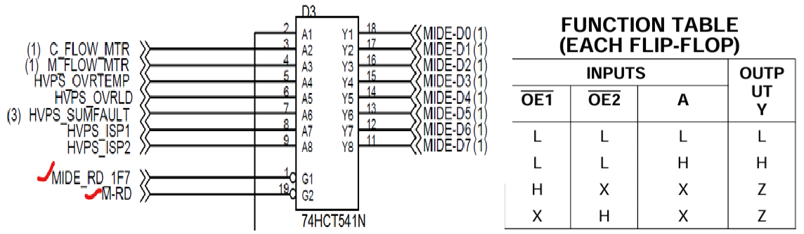
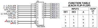
The 3-state control gate is a 2-input AND gate with active-low inputs so that if either output-enable (OE1 or OE2) input is high, all corresponding outputs are in the high-impedance state. The outputs provide noninverted data when they are not in the high impedance state.
To ensure the high-impedance state during power up or power down, OE should be tied to VCC through a pullup resistor; the minimum value of the resistor is determined by the current-sinking capability of the driver.
Probably my following observation/issue is because we did not have a pull up resistor on OE1 and OE2, we do see momentary low at the output, when OE1 is high and OE2 is low for short duration.
In our legacy design, we do use the part.
Recently I came across an observation, while the design happened many years ago, which is the reason i call it as legacy.
As per the truth table, I see that OE1 and OE2 signals have to follow each other for making sure the buffer is active only when both are low.
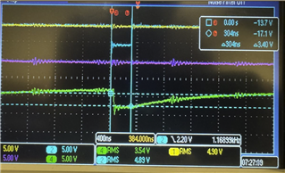
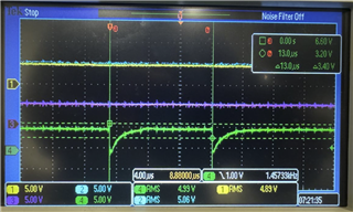
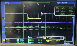
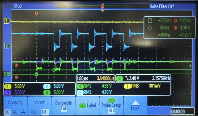
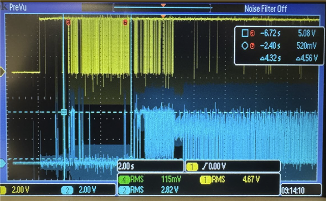
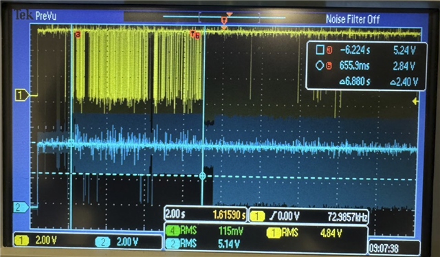
In the following scope captures,
- CH1(Yellow) : OE1 on D3.1, which seems do have constant at 5V level
- CH2(Blue) : OE2 on D3.19, where as CH2 seems to toggle at a rate of 1ms, it goes low for short duration,
- CH3(Purple) : VCC on D3.20, I don’t see major ripple on VCC supply line
- CH4(Green) : MID3 on D3.15, There is change in MID3 signal output, which can false trigger HVPS OVR TEMP, again I believe it depends on the during of low time.
But it is really helpful if you can clarify why MID3 D3.15 signal changes its state for short duration when D3.19 low and D3.1 is high state ?
Is it because we did not have a pull up resistor on OE1 and OE2, we do see momentary low(inverted) at the output, as we did not have the high impedance state set with a pull up resistor in our design?
Can you confirm if we are driving the IC in wrong format, where the expectation is to drive both OE1 and OE2 Low instead we are intermittently(rate of 1ms) driving only OE2 low ?
and also I see this as a major concern to have false triggers of HVPS OVR TEMP signal that's the input of the buffer and MID3 is the output of the buffer.