SN74ALVC164245: TXB0108PWRG4 | TXU0101DRYR | SN74ALVC164245

Part Number: SN74ALVC164245

Tool/software:

Hello,

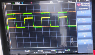
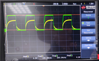
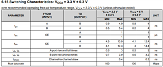
Could I know the the maximum frequency of these level shifters ? At what frequency it will smoothly shift the voltage of the PWM ro clock signals without changing the Rise time and fall time?

  • Hi Amol,

    It is dependent on the output voltage of interest. 
    See FAQ] Can  I estimate Data Rate Frequency not given for my voltage level? as a reference, if the voltage level of interest is not specified in the data sheet, thanks. 

    Best Regards,

    Michael. 

  • Hi Michael,

    In my understanding, Tpd is nothing but the pin to pin delay. i.e. the delay at the output of level shifter in the signal.(input to output)

    Please correct if I am wrong.

    And my question is related to input frequency- see example below -

    I have tested this on TBX eval board - 

    Below waveform shows the input 5V is applied (ampl 2) and output 3.3V (ampl 1) and freq. 20KHz.

    and now frequency at 200KHz, waveform shows the input 5V is applied (ampl 2) and output 3.3V (ampl 1) but if you can see 3.3V output, the rise time got changed, I didn't see the output in the square wave shape. Likewise, if you increase the frequency Rise time will get increased.

    I hope my question is clear. please check and help me to understand the max frequency of level shifter that it can handle.

  • Hi Amol,

    Your understanding is correct.

    However, the delay is an indication of the lumped capacitive load, correlating back to the frequency the output translates. Hence, delay as an estimate.

    TXB can handle 200 kHz just fine, with below specifying up to 50 MHz. Also, if the rise time is above 3.9 ns below, it can further indicate increase in capacitive load. Please help confirm the output's lumped capacitance for both waveforms. thanks.

    Best Regards,

    Michael.