This thread has been locked.
If you have a related question, please click the "Ask a related question" button in the top right corner. The newly created question will be automatically linked to this question.
Tool/software:
Hi Expert,
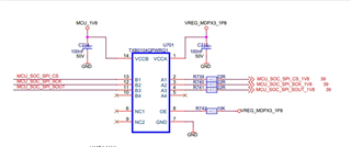
My customer Li-Auto is using this device for level shifting between MCU and SoC in IVI platform. Below is the simplified diagram and schematic:
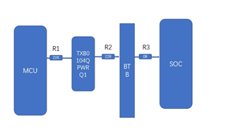
(BTB is a connector.)
The phenomenon is MCU side cannot pass high-level CS signal to SoC side.
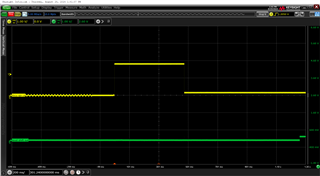
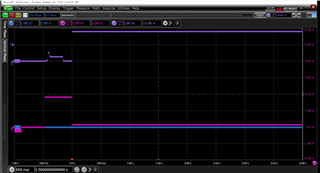
1. Here is the waveform tested when R3 is disconnected. We can see MCU side is driven low after VCCA side is powered up.
bluish-purple line: VREG_MDPX3_1P8
pinkish-purple line: CS signal on R1
blue line: tested on R2
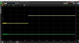
2. If R2 is disconnected, then high-level can be translated to A side.
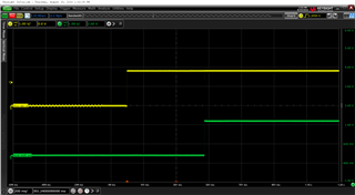
3. If directly connecting R1 and R2 together, then high-level can be passed to SoC side.
Is this related to MCU driving strength?
And seems that the BTB connector affects translating direction.
Can you help to give some suggestions on this?
Best,
Jiahao
The schematic is incomplete. Are there any pull-up or pull-down resistors connected to the CS line? What is the total capacitive load of all traces and connectors?
The waveform looks OK. When the TXB is powered on, both input and output signals are always low.
For unidirectional signals, a unidirectional translator like the TXU0104-Q1 would be a better choice.
Hi Jiahao,
What is R1, R2 and R3 in reference to? Are they different channels or resistors not shown in the schematic?
It seems that this application does not require level shifting, more-so system requiring buffering instead. In which case, the TXU0104-Q1 would be a better fit.
Regards,
Jack
Hi Jack and Clemens,
Thanks for reply.
When the TXB is powered on, both input and output signals are always low.
Customer software decides that MCU pulls CS high before TXB0104 is enabled. Ideally once OE and VCCA side go high, it should appear high-level on SoC side.
What is R1, R2 and R3 in reference to? Are they different channels or resistors not shown in the schematic?
R1, R2 and R3 are series resistors on CS trace from MCU side to SoC side. R739 in schematic is the R2 in diagram. R1 is placed on MCU side, and R3is placed on SoC side. They did not show in this schematic.
Before proposing new device TXU0104-Q1, we want to know why it does not work for TXB0104.
Best,
Jiahao
Here are some additional information and test waveforms from customer.
Capacitive load on MCU side: 2.423pF,
Capacitive load on SoC side: 7.573pF,
Capacitance on BTB: unknown
Customer said if using MCU IO to drive high-level signal, it will be no problem. So, customer thinks they can rule out the possible cause of capacitive loads requirement.
Changing the driving strength of MCU to 12mA (maxmimal strength) also does not work.
Below are some tests:
Test1: Change R2 to 0Ohm
Yellow: MCU CS signal on R1
Green: level shifter output on R2
Same phenomenon, MCU CS signal on R1 is driven low after VCCA power-up, level shifter output keeps low
Test 2: Change R2 to 0Ohm, disconnect R3
Same phenomenon
Test 3: Change R2 to 0Ohm, disconnect BTB
MCU CS signal on R1 keeps high, TXB0104 is not enabled because 1.8V comes from BTB.
Test 4: Disconnect R2
Work normally, level shifter output high after enabled.
Test 5: Add a 2.2uF cap between OE and GND
MCU CS signal on R1 keeps high after VCCA power-up, level shifter output keeps low
From test1-4, I think BTB has some impact on this issue. This seems to trigger the one-shot circuit in wrong direction, which means translating SoC side to MCU side.
For test5, I have no idea why two sides of TXB0104 can appear different voltage level.
Please give some suggestions here, thanks.
Best,
Jiahao
Hi Jiahao,
For all tests, what is the voltage at VCCB?
Customer software decides that MCU pulls CS high before TXB0104 is enabled. Ideally once OE and VCCA side go high, it should appear high-level on SoC side.
Please ensure that both power supplies, VCCA/ VCCB are fully ramped up prior to sending signals.
In the event that OE is driven low or when one power supply, VCCA or VCCB is powered off and at 0V, the I/Os are in a HIGH-Z state cannot influence one another.
From test1-4, I think BTB has some impact on this issue. This seems to trigger the one-shot circuit in wrong direction, which means translating SoC side to MCU side.
TXB is intended to be weak so the I/Os can be overwritten when signal changes direction. With TXU being a fixed translator, this is not an issue since the directionality remains fixed, so it is a more robust solution here.
Regards,
Jack