This thread has been locked.
If you have a related question, please click the "Ask a related question" button in the top right corner. The newly created question will be automatically linked to this question.
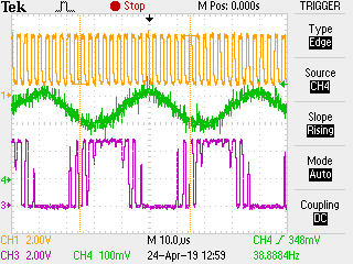
I am using the circuit on data sheet page 17 with timing R =1.2k, timing C = .0015, Rload = 1.2k, C2 = .005. Pin 2 floats at approx 3 volts. In order to get an output at pin 8, I have to pull pin 2 down to 230 mV and apply a 100 mV peak to peak signal to get 0 to 100% duty cycle PWM. Is my application correct?
I would like to correct my statement about pin 8. It is actually low when pin 2 is unmodulated. This changes to high when pin 2 is 0 volts. At approx. 250mV pin 8 has the waveform per fig 19. If a 100mV sinewave is superimposed, then pin 8 turns into a PWM waveform.
Question: is the note VCO terminal (+6%) a reference to pin 2 being approx. 300 mV?
I have attached scope traces of pin 5 yellow, pin 2 green and pin 8 magenta .
Is this what I have been looking for?
It is necessary to deliberately sink current out of pin 2 until pin 8 effectively becomes unstable at around 250 mV. This is somewhat ridiculous and without proper documentation this application is useless.
I have abandoned this chip in favor of Linear Tech LTC6992.