Hi Sirs,
Sorry to bother you.
We have use two TI logic as below, the main application is the frequency division ( ÷ 2).
Could you help review schematic and check is this schematic will suitable for our application?
Thanks!!
Schematic:
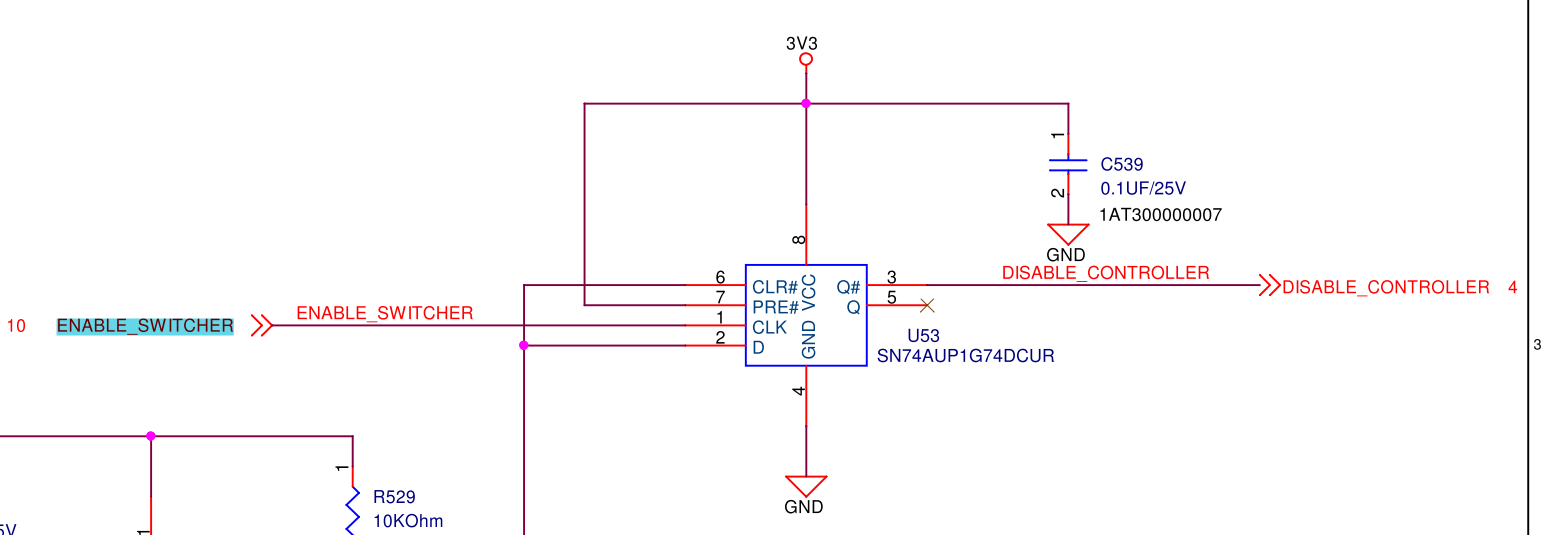
Hi Sirs,
Sorry to bother you.
We have use two TI logic as below, the main application is the frequency division ( ÷ 2).
Could you help review schematic and check is this schematic will suitable for our application?
Thanks!!
Schematic: