This thread has been locked.

If you have a related question, please click the "Ask a related question" button in the top right corner. The newly created question will be automatically linked to this question.

SN74LVC1G175: Using D type Flip-Flop make a Rising edge control power supply

Part Number: SN74LVC1G175
Other Parts Discussed in Thread: SN74HCS74, SN74HCS74-Q1, SN74LVC2G17, , SN74LVC2G14

The target is using a D type Flip-Folp to make a rising edge controled power supply.

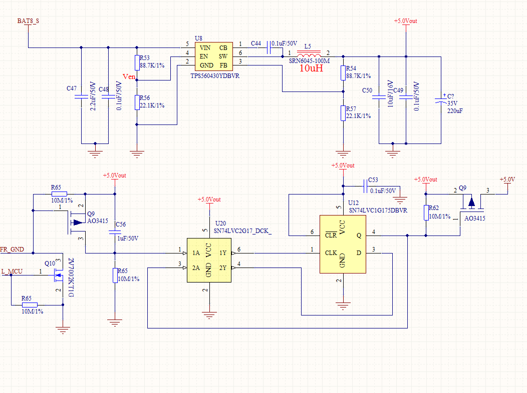
  Here is the Sehematic.

The first status is FR_GND pulled high by R65, Q stay in L so Q9(P mos) close provide 5V (H ) to D.

by ground FR_GND and release this net, we will have a rising edge on CLK of U12 which will turn Q from L to H(the status of D), and then ,the P-mos will open and D turns to L for next operation.

by ground FR_GND and relase again, another rising edge on CLK of U12 will turn Q from H to L.

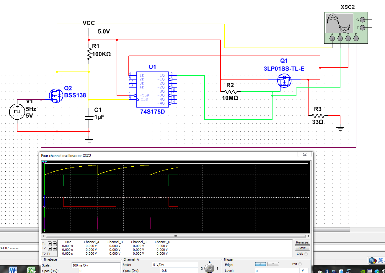
has try this sehematic on multisim simulation and everything just looks fine.

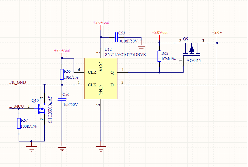
By worried about the possible noise on D of U12, had try to put fillter on control and feedback loop as follow

But the fillter does not help.

For clear, i have try to control the D of U12 maunally like the schematic below.

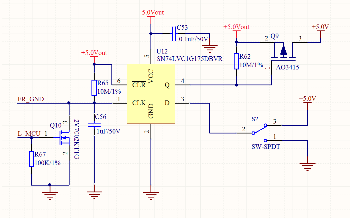
By switching the S? manually to control the status of D, the Q are following the status of D when CLK rising up.

Any suggestion or is there something which can be use to instead of this schematic?

  • Hi,

    My first question is what is the goal with this schematic? My understanding is that you are trying to power an MCU with an external switch while also giving the MCU capability to turn itself off. If this is not the case why can you not just let the MCU drive the PMOS that turns on and off your 5V supply.

    We have the SN74HCS74 that you could possibly use. It has built in schmitt triggers on its inputs which will allow slow and noisy inputs on the device.
    It also has a ~Q output which you could tie directly to your D output. This will allow you to toggle Q without using that PMOS switch.

    Below schematic shows the ~Q being connected directly to D allowing the input switch at the CLK pin to toggle the value at Q.

    Thanks!

    -Karan

  • Hi Bing,

    All of the filtering you are doing will most likely damage the device. CMOS inputs don't like slow edges, see FAQ below:

    https://e2e.ti.com/support/logic/f/151/t/737694?tisearch=e2e-sitesearch&keymatch=faq%3Atrue

    This leads me to my other concern, it seems D will be floating when the Q9 is open since there is nothing shown to drive it low(unless that's another net for a different 5 V supply which would also be an issue if so). 

    Your first schematic will work if you replace the current device with a flip flop with integrated schmitt triggers like the SN74HCS74-Q1 or add external schmitt triggers in front of the CLK input and D input (like the SN74LVC2G17). Schmitt triggers will have some noise rejection of their own so the filtering may not even be required. The HCS74 function will provide you with a Qn output which will eliminate the need of the Q9, also you can tie an RC delay to have a power on reset so the circuit starts up the way you desire.

  • Hi Karan,

    Thank you for your reply.

    unfortunately, It's hard to purchase the part you provide(SN74HCS74) in china.

    looks like i have to use a Dual Schmitt-Trigger instead of one single chip.

    will reply to Dylan of the latest design.

    Thank you for your help , and hoping you will keep watching this case from your side.

    Thank you.

  • Hi Dylan 

    Thank you for your help.

    Since it's very hard to buy SN74HCS74 where i am, i have to use SN74LVC2G17+SN74LVC1G175 to get what i want.

    The goal of this design is :

    Background: this is the power supply circuit to power up a battery manger system. Since this powerd by Battery, there must be a funtion exist that can cut off the power from battery to BMS just in case not destroy the battery when user forgot to charge.

    To let it happen, i need the MCU has the ability to close the power and itself, and also allow users to re-active the power supply from outside with a single wire. At same time, users should not have ability to ingroe this protect funtion for seafty.

    Then battery pack are 8 Li-iron (3.2V) in series which provide about 25.6V normal.

    Here is the updated schematic.

    There is a step-down DC/DC to convert the voltage from 25.6V to 5V with high efficiency and low Iq.(since it's hard to find the logic devices which can work at high volt, and the DC/DC use less than 100uA when have low load)

    By using a dual schmmit trigger, the signal to U12 get buffered and have a very high V/uS ramp.

    So when L_MCU been pulled high or FR_GND pulled down to ground and then release the control, the RC circuit will start to work and get 1A of U20 a falling edge , which will prvoide a rising edge from 1Y of U20 to CLK of U12.

    Is this design work?

    Is there any reason that should not tie D of U12 and +5.0V together?

    Thanks and best regards,

  • Hi,

    Firstly, I believe you meant to you use a SN74LVC2G14 which is a schmitt trigger inverter. The U20 you are using is a buffer and won't invert your signal.

    Secondly, I am unclear on the functionality of your RC circuit. When you pfet turns on, the cap will be bypassed putting the 1A pin of U20 to 5V. If you didn't have a capacitor there, I believe your device would operate with same functionality. When the pfet turns off, the cap becomes an open again immediately because it will get charged by the 5V supply.

    The D is the data pin, it is used to alternate your Q pin on every clock pulse caused by your MCU. I am not sure why you would want to connect it to the supply?

    Thanks!

    -Karan

  • Hi Karan

    Thank you for your reply.

    First, the reason of creating this circuit is:

    1.This is the power suplly for a BMS;

    2.Since the power source are battery, to make sure not over discharger the battery itself, i want the MCU has the capability to turn the power off by itself.( MCU can not turn power on by itself)

    3.There is a wire named FR_GND which are able to be touched by user which can turn system on when MCU does not have power.

    2nd, The reason of RC is :

    1. FR_GND are controled by user, who may not have a quick switch components

    2.Most likely, User will short FR_GND to GND by wire in hands, which may create a series of short/open happen in a very short time. The RC circuit can fillte those quick on/off signal to make sure there is only one rising edge can be sent to CLK pin of the devices.

    I had more test in last couple days, like putting 1k resistor in between 2Y and D and/or Q and 2A. But the U12 has never work as expected. and the DC/DC power supply got damaged once for no reason.

    Is there any suggestion?

  • Hi,

    Have you changed your U20 to an inverter? U12 will not work unless D pin goes through an inverter.  Secondly, I am saying I don't believe your RC circuit is built correctly. It will not do what you are intending. Your PFET will bypass that capacitor in your RC and when the PFET turns off, the capacitor cannot discharge because of its placement. You mean to switch the location of the resistor and capacitor in your RC circuit.

    Thanks!

    -Karan

  • Hi Karan Thank you for your reply. Forgive me if I have spent error since this reply are finished by my cell phone. 1st. Yes I did change U20 to a Schmitt trigger inverter. 2. I think the RC circuit should work. When p mosfet on, the cap will discharge to zero volt. By the time that p mosfet turns off, the cap C57 will starting to charger thru the resistor under knees of the cap. The voltage between cap and resistor is going down from 5V to zero volt which create a fall edge, and a rising edge will be created by inverter on the output side of the inverter. So this should work.
  • Hi,

    I believe the C56 will not discharge when the pfet is on because your 5V supply will also provide current. The capacitor when fully charged is an open. So if anything the node between the resistor and the capacitor will go from 0V to 5V causing a positive edge when the pfet is turned on.

    You should take scope shots at pin 1A of U20 and pin 4(Q) of U12. This will provide you with exactly what you need to know of where your circuit is failing.

    Thanks!

    -Karan

  • Hi Karan.

    Sorry for the late of reply .

    I had this circuit printed on board and tested.

    The issue i have is i had wrong opinion of U20 which is a buffer , ( i used that as a inverter).

    Now, Everything just work as it is.

    Thank you .