


Other Parts Discussed in Thread: SN74HC08, SN74HCS08-Q1
Dear team,
Recently my customer uses this device, and he found that there are 25pcs chips failed when he tested them. The fault phenomenon of the most chips is that pin3 & pin8 & pin11 short to GND, and several chips is that pin3 & pin8 & pin11 & VCC short to GND, and other several chips is that the resistance between pin3 & pin8 & pin11 and GND becomes smaller.
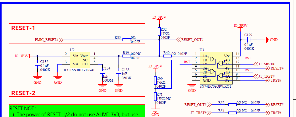
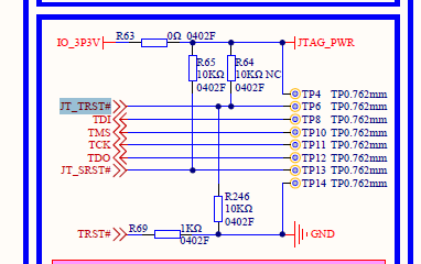
The schematic is as below, second channel is unused.
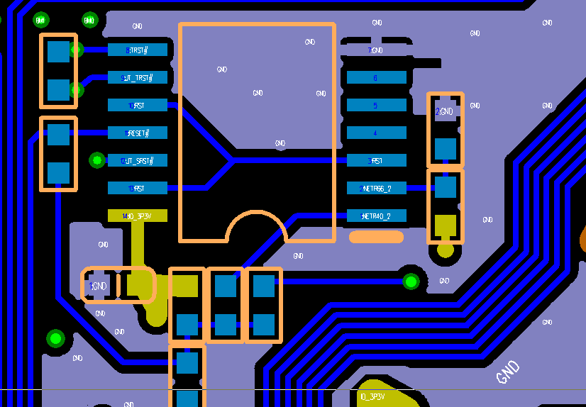
The layout is as below,
The waveform of output when power on,
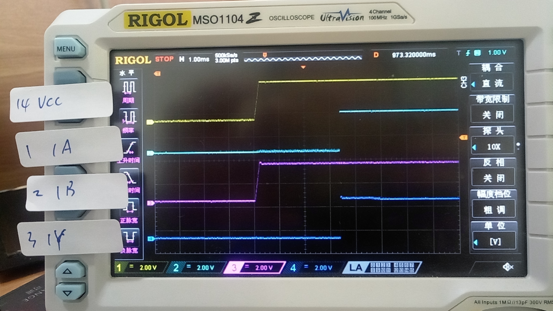
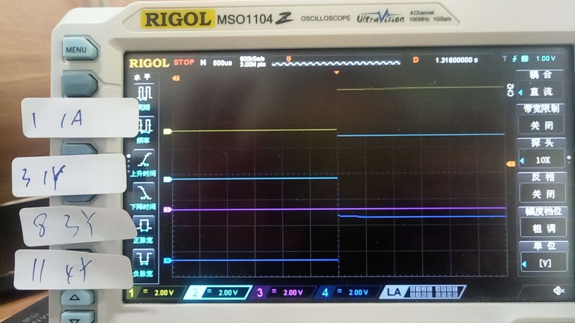
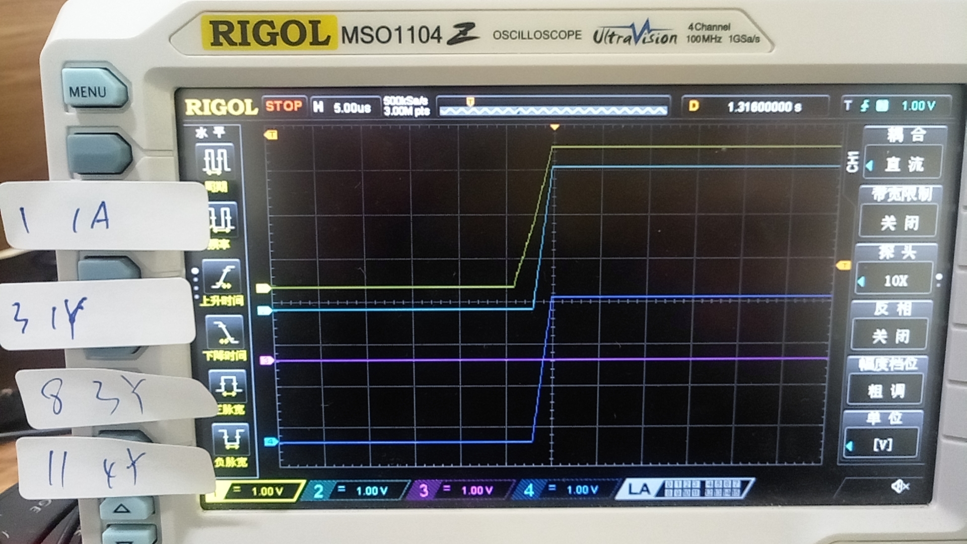
The waveform of output when power down,
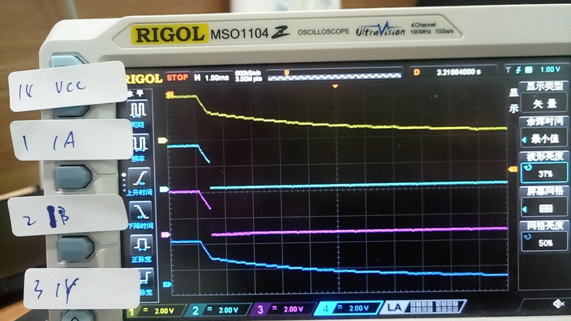
According to above waveform, the voltages of input and output when power on/power down don't exceed absolute maximum voltage 7V, but the customer violated two rules as below,
1. unused input pin should be connected to VCC/GND, but the customer just floated them(pin4 & pin5)
2. the input transition rise time is 2500ns which exceeds to the max recommended value
But I'm not sure whether above 2 items will result in this fault. Could you please help analyse this problem?

Thanks & Best Regards,
Sherry

