This thread has been locked.

If you have a related question, please click the "Ask a related question" button in the top right corner. The newly created question will be automatically linked to this question.

SN74LVC2G17-Q1: SC70 package layout

Part Number: SN74LVC2G17-Q1

Hi Team,

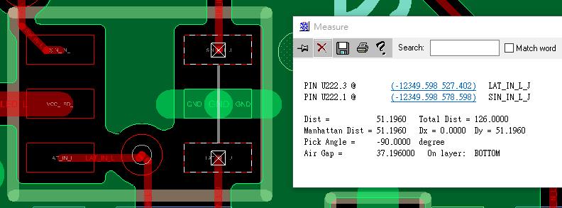
According to datasheet, the package is 2.2mm*1.3mm instead of 1.9mm*1.33. Could you let me know if this difference is critical?

12424.402-12349.598=74.804mil=1.9mm

578.598-527.402=51.196mil=1.3mm

Regards,

Roy

  • According to the datasheet, the package size can be anywhere between 1.85 mm × 1.10 mm and 2.15 mm × 1.40 mm.

    The pin pitch is 0.65 mm, so the distance between the centers of the outermost two pads should be exactly 1.3 mm.

    The outer edges of the pins can be anywhere between 1.80 mm and 2.40 mm apart. The centers of the pads are 2.2 mm apart because the pads are larger than the pins to allow for better soldering.