This thread has been locked.
If you have a related question, please click the "Ask a related question" button in the top right corner. The newly created question will be automatically linked to this question.
Hi Team,
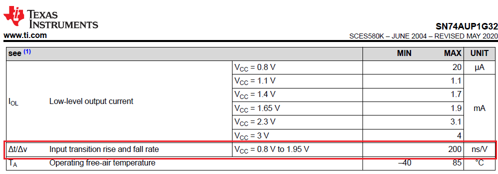
Our customer is confusing about the input transition rise and fall rate specification( Δt/Δv ) in the datasheet for SN74AUP1G32, as the usual understanding, the input voltage transition slew rate should be limited in V/us, but looks like we recommended the fast the better for this spec in datasheet with maximum 200ns/V. Can you help to clarify this spec? Does it mean 0 to 1V input voltage transient should be no more than 200ns?
Thanks.
The slew rate and the rise/fall rate describe the same thing, the slope of signal edges. One uses time divided by voltage, the other, voltage divided by time. They are simply the reciprocal of each other: 1 / (200 ns/V) = 5 V/µs.
The datasheet requires a maximum rise/fall rate, which is the same as a minimum slew rate.
This limit prevents the effects described in [FAQ] How does a slow or floating input affect a CMOS device?