This thread has been locked.

If you have a related question, please click the "Ask a related question" button in the top right corner. The newly created question will be automatically linked to this question.

SN74ALVC244: The output distortion of SN74ALVC244

Part Number: SN74ALVC244

Hi team,

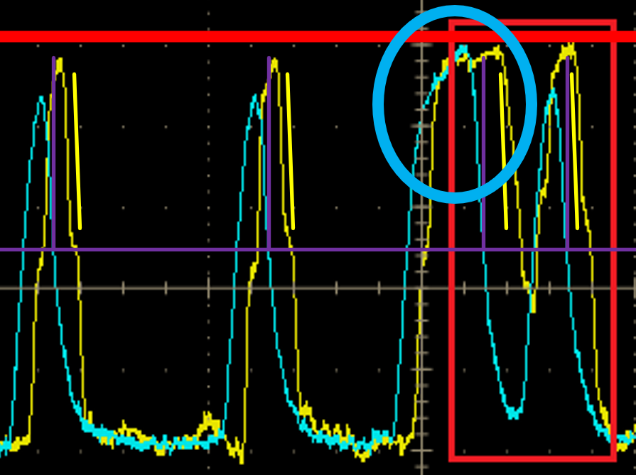
My customer is using the SN74ALVC244PWR now as 125M buffer, we find the output waveform has some distortions(blue is input A0, yellow is output Y0), Whether it's because the parasitic cap? Do you have some ideas? Thanks.
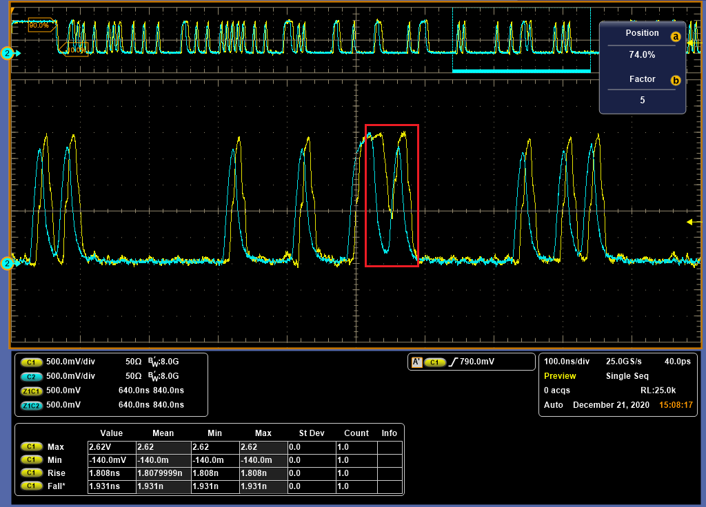
  • Hi Frank,

    I added a few things to make it easier for comparison of waveforms.

    (1) Purple lines show the 50% input voltage level and the falling edges of each waveform crossing it. These are used for timing.

    (2) Yellow lines are the same slope, for comparison of the falling edges.

    (3) Red line at the top is just above the maximum voltage (assuming 2.5V supply)

    (4) Blue circle indicates the extended waveform.

    -

    Looking closely at the waveforms, the first thing I notice is that the output rising and falling edges have several changes in transition rate, which typically indicates a transmission line loading with some reflections (probably 12cm+ in length).  I also notice that the input signal isn't reaching the supply value in most pulses (the first two only get to ~2.2V, while the third makes it to ~2.5V. The output reaches a higher voltage, but also doesn't make it to the supply on the first two pulses, but does get to the supply value on the third and fourth. Additionally, it looks like there's a significant amount of noise in the system, with the ground varying by about 150mV.

    My purple line (horizontal) is the midpoint voltage (1.25V), which I drew vertical lines up for the falling edge. You can see a consistent delay on the rising and falling edges of the first two waveforms in my image. of ~10ns, which tells me that the capacitive loading is much heavier than the timing values provided in the datasheet (30pF @ 2.5V supply). This is probably just due to a long trace and it's associated parasitics.

    The third pulse has a similar rising edge to the others, but the output takes nearly twice as long to react as with the other pulses -- which is the issue I assume the customer is concerned with. I also see that the falling edge of that signal is slower than the others (note the difference between the slope of my yellow line and the falling edge).

    If there are no changes in the system during that falling edge, then this is most likely a combination of noise on the supply and reflections at the output.

    -

    Can we ask for two things:

    (1) Details on the loading, ideally a schematic, and layout.  I'm specifically looking for the trace length, geometry, # of vias, and other devices connected to the output.

    (2) Another scope shot showing the issue at a lower time scale (10ns / div). I would also like to see a 'good' pulse at the same scale.