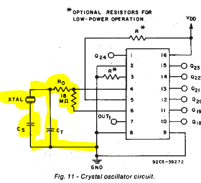
I am referring to the CD4521B (CMOS 24 stage Frequency Divider) TI Datasheet Copyright 2003 (Page 3-286), figures 10 and 11 and I have the following questions:
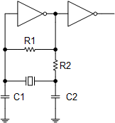
Q1. Does the oscillator frequency calculation formula given under fig.10 also apply to the oscillator circuit in fig11?
Q2. How to calculate the capacitor "Cs" value shown in fig.11?
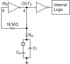
Q3. In fig. 11, an unannotated resistor between pin 4 and pin 6 is shown. Is this the resistor "Rt"?
Q4. Is the resistor "R0" shown in Fig.11 has the same functionality as resistor "Rs" in fig.10?
If so, then, since "R0 = 18 MOhm" (as shown in fig.11), can one use the relationship "Rs >= 2Rt" (as given in fig. 10) to calculate the value of the unannotated resistor in fig.11 (presuming, it is "Rt")?