Other Parts Discussed in Thread: CD40106B
Dear all,
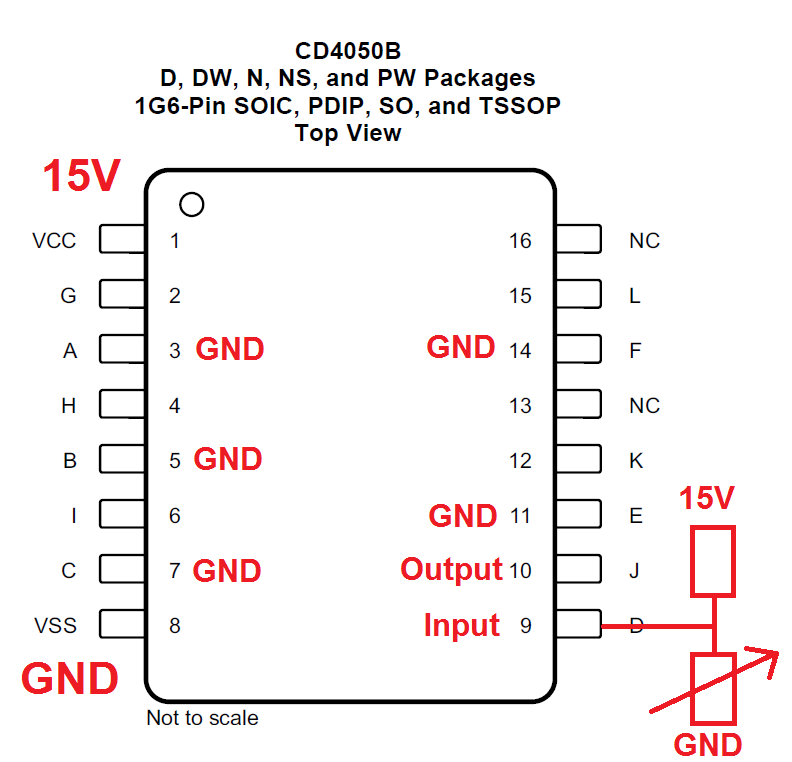
I am trying to properly understand the datasheet of the CD4050B Hex Buffer IC. It is supplied with 15V and decoupled with a 100nF (not shown in the schematic). Input D (pin 9) is connected to a potentiometer such that a voltage between 0V and 15V is applied to pin 9. On pin 10, I measure the output depending on its input (pin 9). the purpose is to see the threshold voltages at which the output changes its state.
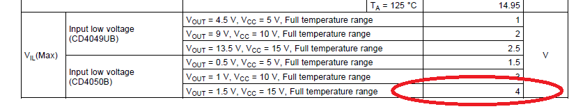
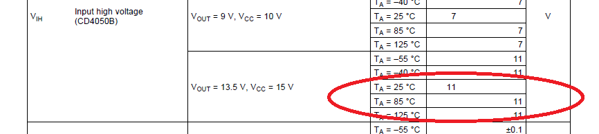
My understanding according to the datasheet (Table 6.5):
Output change from high to low:
When input voltage is below 4V
Output change from low to high:
When input voltage is 11V
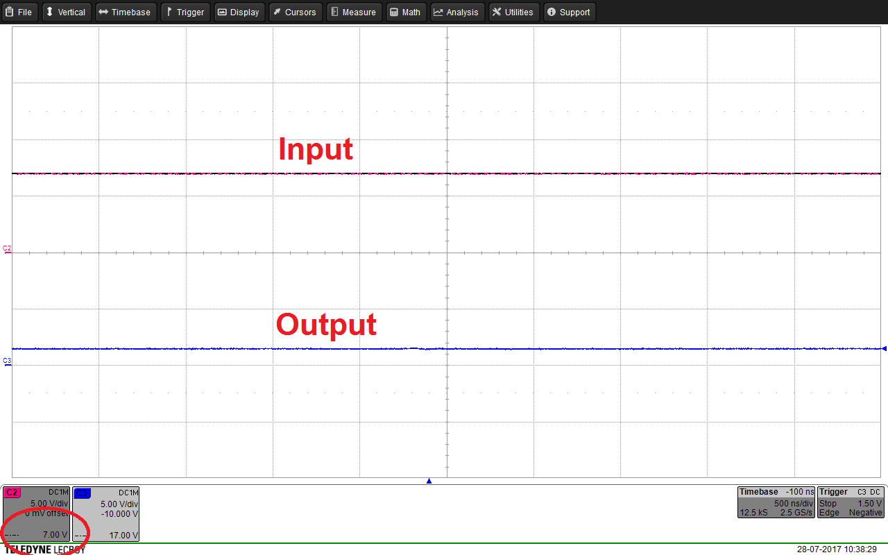
My measurements, however, show that at 7V on the input, the output changes its state (for both low to high scenario and high to low scenario). This would mean that there is no hysteresis behavior on the CD4050B IC.
Am I correct in my understanding that the CD4050B does not have a hysteresis like behavior? If so, how can I interpret the values from Table 6.5 then?
Thank you.
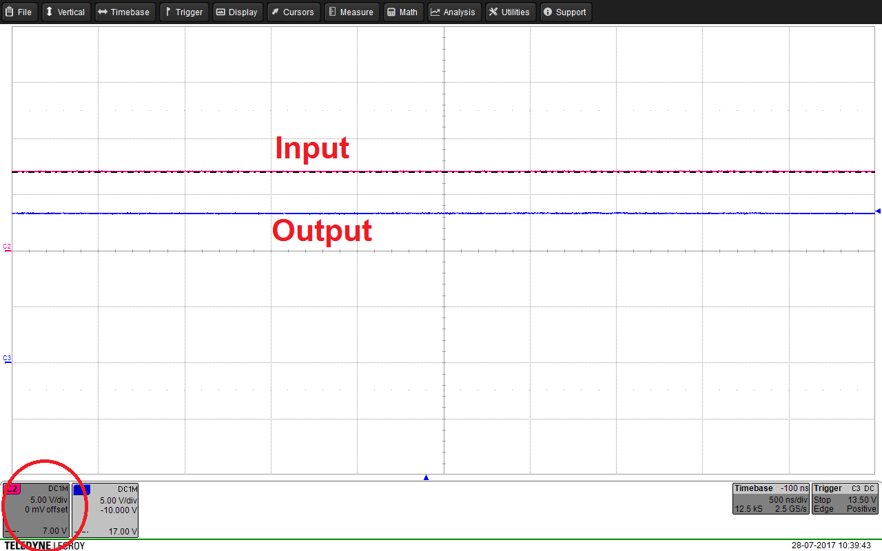
Below the relevant graphs: