This thread has been locked.

If you have a related question, please click the "Ask a related question" button in the top right corner. The newly created question will be automatically linked to this question.

LSF0204: LSF0204 - Minimizing Leakage Currents

Part Number: LSF0204
Other Parts Discussed in Thread: LSF0108, SN74LVC2G07, LSF0102, TINA-TI, SN74LVC1G07

Hello TI Logic Forum,

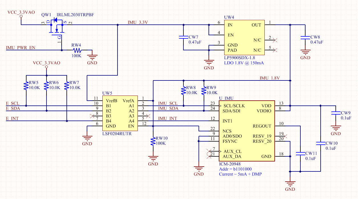
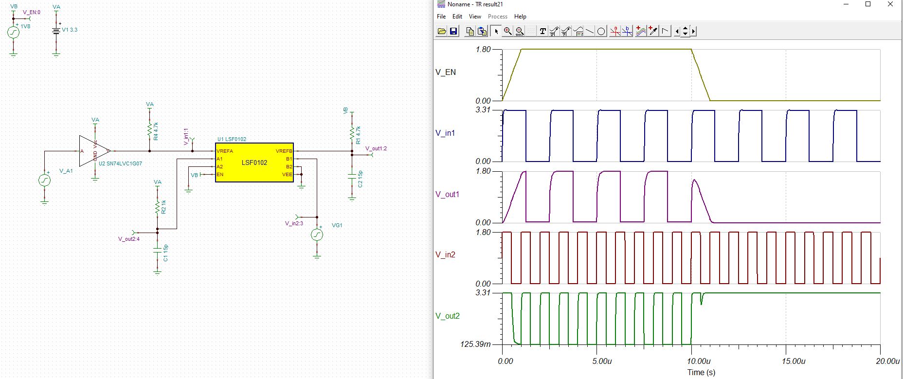
I need to translate an I2C bus and control signal between a 3.3V "Always On" processor and a 1.8V peripheral device that will often be powered off.  Reading through other forum posts on the LSF0204, engineers reported significant parasitic power leakage between the A and B ports (with up to 1V appearing on the unpowered rail) due to the 200K internal resistor on Vref_B and general input leakage.  That's highly undesirable for my design.  I noticed that Ioff is only specified under the condition that Vref_A = Vref_B = 0 and not for a single unpowered port.  So rather than simply disabling the 1.8V LDO and Vref_A of the LSF0204 with the IMU_PWR_EN signal, I'm proposing to also remove power from Vref_B using the NMOS FET at the top left of the schematic.  Will that minimize the leakage and is there any downside to this approach that I'm overlooking?

Thanks,

Steve C

  • Hey Steve,

    I think you can do this, but there are a couple things to be aware of.

    First, the bias current for the LSF0204 flows into the VrefB port and out of the VrefA port -- with 3.3V and 1.8V you're looking at about 3.5uA of current coming out of pin 1 of the LSF0204.  The 100kohm resistor will soak up (1.8/100k = ) 18uA, so that shouldn't be a problem, but it is something you should be aware of. Removing the 100k could result in the LDO failing to regulate properly (ie current flowing back into an LDO is usually bad).

    When QW1 is disabled, no current can flow that way, so the 0.47uF capacitor will discharge through the LSF0204 and into the regulator. Given ~300kohm between the capacitor and ground, I would expect that discharge to take quite a while if only the LSF is doing the work -- time constant is  (0.47u * 300k =) 141ms. The other device will probably drain it faster, but you might want to check on just how fast that will happen.

    If the speed of discharge is good enough, then I think this setup is fine.  If there's any residual charge on VrefA or VrefB, ie either of them isn't at 0V, then we can't guarantee isolation between the A and B sides of the device.

    There are a couple of other options of how you could achieve the same thing. The LSF0204 is different from the rest of the LSF family in that it adds some control circuitry to handle the enable pin. With the other devices, (any LSF01xx) you get direct access to the gates in the device and thus can directly shut off the channels at any time.

    One option:

    With the LSF0108, you could setup the circuit the way it usually is - 200kohm resistor for bias + pull-ups only on appropriate channels, and then use an open-drain driver to force the EN pin low when either supply is off. You can tie two open-drain buffers (SN74LVC2G07) together at the output directly to the EN pin, and if either output goes low, the whole device will be forced into a high-impedance state. The SN74LVC2G07 would be powered by the 1.8V supply -- it supports over-voltage inputs, so 3.3V on one channel would be fine.

    Another option:

    The LSF0102 can be used as a 3-channel voltage clamp.  To do that, you just need to make a few changes

    (1) The EN pin completely controls the device and is tied to the lower voltage supply - so you would just connect EN directly to 1.8V. I would also add a pull-down resistor to ensure it gets dragged down to 0V when 1.8V is removed.

    (2) Pull-up resistors would have to be added to both sides of the device for all channels. Since the clamp voltage is no longer controlled by a nice bias circuit, the pull-ups are required to reach the appropriate 'high' state voltages on both sides and not just on the 'high' side (3.3V side).

    (3) The 'VrefA - VrefB" pins would act as your third channel. The performance is identical to the other channels - usually we just use these to setup the bias, but here we're not doing that, so you can use the extra channel for data.

  • Hi Emrys,

    Thanks much for the detailed response.  It is that bias current flowing from Vref_B to Vref_A that I'm trying to eliminate in the partial powerdown state, which is why I inserted QW1.  Your 2nd option of using the LSF0102 as a 3-channel translator is interesting.  It's certainly not obvious from the datasheet that it can be used that way.  If I understand correctly, that option would eliminate the need to remove the high-side (3.3V) voltage as long as the gates (EN) were tied to the low-side supply (1.8V).  I could then remove the QW1 FET and have the always on Micro control the 1.8V LDO as shown (I omitted a pullup on IMU_INT since it is a push-pull output from U_IMU).  With it wired this way am I correct in interpreting that, with the LDO disabled, the input leakage currents from the 3.3V side should be limited to IIH @ EN=0, or 5 uA Max per pin?

    Thanks again,

    Steve C

  • Yes, the datasheet is really written to help our customers to use the device in one particular way and to avoid complex questions as much as possible.

    There's one more thing you need to add in this configuration - you'll need a pull-up resistor from B2 to 1.8V.

    The EN pin will clamp all channels to approximately 1V, after which the pull-up resistors will take over pulling the outputs to the appropriate voltage.

    You will probably need to reduce the pull-up values a bit also. 

    One method is to just build a prototype and adjust the pull-up resistors until everything works.  I'd start with 4.7k on the I2C lines and 1k on the INT line.

    If you want to calculate the values first, you need the total parasitic capacitance on each side of the device, the maximum sink current of the drivers (on both sides of the LSF) and the desired max data rate of each signal.  From the equations you should get a range of resistor values, and I would usually pick them to be as large as possible while still meeting the speed requirements to reduce power consumption and improve V_OL specs.

    There's a video with more details here: https://training.ti.com/translation-lsf-family-0?context=1134826-1139264-1134794 

  • I threw together a simulation in Tina-TI so you can mess with it a bit if you like.

    I used the SN74LVC1G07 to simulate the open-drain output of the I2C protocol -- your driver will probably be weaker than that, so you might want to add a series resistor (maybe 50 ohms?) to that line to make it more realistic.

    Screen capture:

    Simulation file:

    LSF0102_clamp_ex.TSC

  • Hi Emrys,

    That's very helpful, thank you.  In your previous post you stated that I would need a pullup on the B2 pin of my revised schematic.  In my circuit, the IMU_INT signal connected to B2 of the LSF0102 is actually a push-pull output of U_IMU so that signal is being "up-translated" to 3.3V. 

    Regards,

    Steve C

  • Ah, I understand. If it's a unidirectional signal, then you can ignore the pull-up. That's only required if the direction changes.