Part Number: AM2434
Customer asking which design guide they should follow in the datasheet.
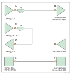
Do we need to control LBCLK and DQS length for QSPI?
They are planning to use S25HS512TFANHI013(same as EVM’s one, 1.8Vversion)
Part Number: AM2434
Customer asking which design guide they should follow in the datasheet.
Do we need to control LBCLK and DQS length for QSPI?
They are planning to use S25HS512TFANHI013(same as EVM’s one, 1.8Vversion)