This thread has been locked.

If you have a related question, please click the "Ask a related question" button in the top right corner. The newly created question will be automatically linked to this question.

TM4C1233E6PM: Incorrect reading on ADC

Part Number: TM4C1233E6PM
Other Parts Discussed in Thread: SEGGER

Tool/software:

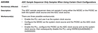
I have been facing an issue with ADC channel 11 on the tm4c12433 MCU. I am consistently reading a raw value (step count) of 890, even when no voltage is applied. Ideally, it should read zero as a raw value.

Here are the details:
- **MCU:** tm4c12433
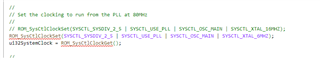
- **Crystal Oscillator (Xtal):** 6 MHz

I have ensured that the pins are correctly enabled as ADC. Below is the configuration I am using to read from ADC channel 11:

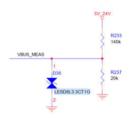
#define VBUS_MEAS_ADC_BASE GPIO_PORTB_BASE
#define VBUS_MEAS_ADC_PIN GPIO_PIN_5

GPIOPinTypeADC(VBUS_MEAS_ADC_BASE, VBUS_MEAS_ADC_PIN);
GPIOPinTypeGPIOInput(VBUS_MEAS_ADC_BASE, VBUS_MEAS_ADC_PIN);

uint32_t uiReadVbusVoltage(void)
{
uint32_t ADCValues[1];

ADCSequenceConfigure(ADC0_BASE, 3, ADC_TRIGGER_PROCESSOR, 0);
ADCSequenceStepConfigure(ADC0_BASE, 3, 0, ADC_CTL_CH11 | ADC_CTL_IE | ADC_CTL_END);
ADCSequenceEnable(ADC0_BASE, 3);
ADCIntClear(ADC0_BASE, 3);


while(1)
{
//
// Trigger the ADC conversion.
//
ADCProcessorTrigger(ADC0_BASE, 3);

//
// Wait for conversion to be completed.
//
while(!ADCIntStatus(ADC0_BASE, 3, false))
{
}

//
// Clear the ADC interrupt flag.
//
ADCIntClear(ADC0_BASE, 3);

//
// Read ADC Value.
//
ADCSequenceDataGet(ADC0_BASE, 3, ADCValues);


SEGGER_RTT_printf(0, "Raw sample (ADCValues[0]): %04d\r", ADCValues[0]);


//
// This function provides a means of generating a constant length
// delay. The function delay (in cycles) = 3 * parameter. Delay
// 250ms arbitrarily.
//
SysCtlDelay(80000000 / 12);
}
}

The Output is printed as below:
Raw sample (ADCValues[0]): 0891

Could you please help me identify what might be causing this issue?

  • Hi,

      I try AIN11 on the LaunchPad and I cannot reproduce your result. Why don't you try my code first on a LaunchPad and then on your custom board. I tie PB5 (AIN11) to either GND or 3.3V and I can see the ADC value equal to either 0 or 4095. 

    #include <stdbool.h>
    #include <stdint.h>
    #include "inc/hw_memmap.h"
    #include "driverlib/adc.h"
    #include "driverlib/gpio.h"
    #include "driverlib/pin_map.h"
    #include "driverlib/sysctl.h"
    #include "driverlib/uart.h"
    #include "utils/uartstdio.h"
    
    //*****************************************************************************
    //
    //! \addtogroup adc_examples_list
    //! <h1>Single Ended ADC (single_ended)</h1>
    //!
    //! This example shows how to setup ADC0 as a single ended input and take a
    //! single sample on AIN11/PE3.
    //!
    //! This example uses the following peripherals and I/O signals.  You must
    //! review these and change as needed for your own board:
    //! - ADC0 peripheral
    //! - GPIO Port E peripheral (for AIN11 pin)
    //! - AIN11 - PE3
    //!
    //! The following UART signals are configured only for displaying console
    //! messages for this example.  These are not required for operation of the
    //! ADC.
    //! - UART0 peripheral
    //! - GPIO Port A peripheral (for UART0 pins)
    //! - UART0RX - PA0
    //! - UART0TX - PA1
    //!
    //! This example uses the following interrupt handlers.  To use this example
    //! in your own application you must add these interrupt handlers to your
    //! vector table.
    //! - None.
    //
    //*****************************************************************************
    
    //*****************************************************************************
    //
    // This function sets up UART0 to be used for a console to display information
    // as the example is running.
    //
    //*****************************************************************************
    void
    InitConsole(void)
    {
        //
        // Enable GPIO port A which is used for UART0 pins.
        // TODO: change this to whichever GPIO port you are using.
        //
        SysCtlPeripheralEnable(SYSCTL_PERIPH_GPIOA);
    
        //
        // Configure the pin muxing for UART0 functions on port A0 and A1.
        // This step is not necessary if your part does not support pin muxing.
        // TODO: change this to select the port/pin you are using.
        //
        GPIOPinConfigure(GPIO_PA0_U0RX);
        GPIOPinConfigure(GPIO_PA1_U0TX);
    
        //
        // Enable UART0 so that we can configure the clock.
        //
        SysCtlPeripheralEnable(SYSCTL_PERIPH_UART0);
    
        //
        // Use the internal 16MHz oscillator as the UART clock source.
        //
        UARTClockSourceSet(UART0_BASE, UART_CLOCK_PIOSC);
    
        //
        // Select the alternate (UART) function for these pins.
        // TODO: change this to select the port/pin you are using.
        //
        GPIOPinTypeUART(GPIO_PORTA_BASE, GPIO_PIN_0 | GPIO_PIN_1);
    
        //
        // Initialize the UART for console I/O.
        //
        UARTStdioConfig(0, 115200, 16000000);
    }
    
    //*****************************************************************************
    //
    // Configure ADC0 for a single-ended input and a single sample.  Once the
    // sample is ready, an interrupt flag will be set.  Using a polling method,
    // the data will be read then displayed on the console via UART0.
    //
    //*****************************************************************************
    int
    main(void)
    {
    #if defined(TARGET_IS_TM4C129_RA0) ||                                         \
        defined(TARGET_IS_TM4C129_RA1) ||                                         \
        defined(TARGET_IS_TM4C129_RA2)
        uint32_t ui32SysClock;
    #endif
    
        //
        // This array is used for storing the data read from the ADC FIFO. It
        // must be as large as the FIFO for the sequencer in use.  This example
        // uses sequence 3 which has a FIFO depth of 1.  If another sequence
        // was used with a deeper FIFO, then the array size must be changed.
        //
        uint32_t pui32ADC0Value[1];
    
        //
        // Set the clocking to run at 20 MHz (200 MHz / 10) using the PLL.  When
        // using the ADC, you must either use the PLL or supply a 16 MHz clock
        // source.
        // TODO: The SYSCTL_XTAL_ value must be changed to match the value of the
        // crystal on your board.
        //
    #if defined(TARGET_IS_TM4C129_RA0) ||                                         \
        defined(TARGET_IS_TM4C129_RA1) ||                                         \
        defined(TARGET_IS_TM4C129_RA2)
        //
        // Note: SYSCTL_CFG_VCO_240 is a new setting provided in TivaWare 2.2.x and
        // later to better reflect the actual VCO speed due to SYSCTL#22.
        //
        ui32SysClock = SysCtlClockFreqSet((SYSCTL_XTAL_25MHZ |
                                           SYSCTL_OSC_MAIN |
                                           SYSCTL_USE_PLL |
                                           SYSCTL_CFG_VCO_240), 20000000);
    #else
        SysCtlClockSet(SYSCTL_SYSDIV_10 | SYSCTL_USE_PLL | SYSCTL_OSC_MAIN |
                       SYSCTL_XTAL_16MHZ);
    #endif
    
        //
        // Set up the serial console to use for displaying messages.  This is
        // just for this example program and is not needed for ADC operation.
        //
        InitConsole();
    
        //
        // Display the setup on the console.
        //
        UARTprintf("ADC ->\n");
        UARTprintf("  Type: Single Ended\n");
        UARTprintf("  Samples: One\n");
        UARTprintf("  Update Rate: 250ms\n");
        UARTprintf("  Input Pin: AIN11/PE3\n\n");
    
        //
        // The ADC0 peripheral must be enabled for use.
        //
        SysCtlPeripheralEnable(SYSCTL_PERIPH_ADC0);
    
        //
        // For this example ADC0 is used with AIN11 on port B5.
        // The actual port and pins used may be different on your part, consult
        // the data sheet for more information.  GPIO port E needs to be enabled
        // so these pins can be used.
        // TODO: change this to whichever GPIO port you are using.
        //
        SysCtlPeripheralEnable(SYSCTL_PERIPH_GPIOB);
    
        //
        // Select the analog ADC function for these pins.
        // Consult the data sheet to see which functions are allocated per pin.
        // TODO: change this to select the port/pin you are using.
        //
        GPIOPinTypeADC(GPIO_PORTB_BASE, GPIO_PIN_5);
    
        //
        // Enable sample sequence 3 with a processor signal trigger.  Sequence 3
        // will do a single sample when the processor sends a signal to start the
        // conversion.  Each ADC module has 4 programmable sequences, sequence 0
        // to sequence 3.  This example is arbitrarily using sequence 3.
        //
        ADCSequenceConfigure(ADC0_BASE, 3, ADC_TRIGGER_PROCESSOR, 0);
    
        //
        // Configure step 0 on sequence 3.  Sample channel 0 (ADC_CTL_CH0) in
        // single-ended mode (default) and configure the interrupt flag
        // (ADC_CTL_IE) to be set when the sample is done.  Tell the ADC logic
        // that this is the last conversion on sequence 3 (ADC_CTL_END).  Sequence
        // 3 has only one programmable step.  Sequence 1 and 2 have 4 steps, and
        // sequence 0 has 8 programmable steps.  Since we are only doing a single
        // conversion using sequence 3 we will only configure step 0.  For more
        // information on the ADC sequences and steps, reference the datasheet.
        //
        ADCSequenceStepConfigure(ADC0_BASE, 3, 0, ADC_CTL_CH11 | ADC_CTL_IE |
                                 ADC_CTL_END);
    
        //
        // Since sample sequence 3 is now configured, it must be enabled.
        //
        ADCSequenceEnable(ADC0_BASE, 3);
    
        //
        // Clear the interrupt status flag.  This is done to make sure the
        // interrupt flag is cleared before we sample.
        //
        ADCIntClear(ADC0_BASE, 3);
    
        //
        // Sample AIN11 forever.  Display the value on the console.
        //
        while(1)
        {
            //
            // Trigger the ADC conversion.
            //
            ADCProcessorTrigger(ADC0_BASE, 3);
    
            //
            // Wait for conversion to be completed.
            //
            while(!ADCIntStatus(ADC0_BASE, 3, false))
            {
            }
    
            //
            // Clear the ADC interrupt flag.
            //
            ADCIntClear(ADC0_BASE, 3);
    
            //
            // Read ADC Value.
            //
            ADCSequenceDataGet(ADC0_BASE, 3, pui32ADC0Value);
    
            //
            // Display the AIN11 (PE3) digital value on the console.
            //
            UARTprintf("AIN11 = %4d\r", pui32ADC0Value[0]);
    
            //
            // This function provides a means of generating a constant length
            // delay.  The function delay (in cycles) = 3 * parameter.  Delay
            // 250ms arbitrarily.
            //
    #if defined(TARGET_IS_TM4C129_RA0) ||                                         \
        defined(TARGET_IS_TM4C129_RA1) ||                                         \
        defined(TARGET_IS_TM4C129_RA2)
            SysCtlDelay(ui32SysClock / 12);
    #else
            SysCtlDelay(SysCtlClockGet() / 12);
    #endif
        }
    }
    

  • Hi,

    Thanks for the reply.
    Sorry, I don't have launch pad right at the moment. But I can show you the adc schematic below.
    I followed the same adc configuration as mentioned in your reply.


    VBUS_MEAS is connected to PB5 (Pin 57) to the controller. When I apply 5V to the R233, I can measure 0.64V on VBUS_MEAS with multimeter. But the raw value read on the pin is 1450 which is 1.16V. When I disable 5V, I can measure 0V with multimeter, but ADC RAW value read as 890 which is equivalent to 0.712 V.

    I have desoldered the R233 from the board to see the changes. I able measure 0V with multimeter, But still the ADC raw value I am reading is 890 i.e 0.71 V.
    And this behavior is same with all the custom boards I have.

  • Hi,

      Did you run my code as is without modification and get the same result?

      Did you use PLL as the clock source for the ADC or you use either MOSC or PIOSC as the source for the ADC? See below errata. I want to know if you are hitting the errata. In my example, I use PLL as the system clock source for the device. 

  • I have configured the code with below clock set

  • Again, when you run my code as-is, do you get the same result? I don't see a problem measuring either 0 or 3.3V when I run the code on a LaunchPad. 

    For experiment, why don't you remove the ESD protection LESD8L3. Does it make a difference?

  • Hi,

    1. I don't have launch pad to test the code. But same adc configuration implemented in my custom board. Still I can measure the RAW adc sample output as 890 steps.
    2. So, as you mentioned, I have removed ESD protection LESD8L3. But still the behavior is same. Raw count is 890 steps.
    3. So I have shorted the LESD8L3 after removing it (ADC line pull downed). With this, I measured steps between 0 to 8 steps count. 

  • Hi,

      Can you repeat the same issue on all of your boards?

    3. So I have shorted the LESD8L3 after removing it (ADC line pull downed). With this, I measured steps between 0 to 8 steps count. 

    Looks like there is some influence by your external circuitry. 

      If you disconnect all components to the ADC input (e.g. the ESD diode, the voltage divider resistors) and simply input a fixed voltage (e.g. 0V, 3.3V and 1.65V), what do you get? I want to know if your earlier results were influenced by the external circuitry,

  • I have disconnected all the components to the ADC input. Now it is reading 2379 raw step count.

    So I have connected 0.128 V to the ADC line. The step count I read is 160.

  • I have disconnected all the components to the ADC input. Now it is reading 2379 raw step count.

    Hi,

      What voltage did you apply to get 2379? Please note that the reference voltage is 3.3V. Therefore, 2379 / 4096 * 3.3 is about 1.91V. If this is what you apply to the input then it is correct. 

    So I have connected 0.128 V to the ADC line. The step count I read is 160.

    160 / 4096 * 3.3 is about 0.128V. I think ADC is correct here. 

  • No voltage is applied while I measured 2379 step count. The ADC pin is open (I have disconnected all the components to the ADC input.

    I don't have the launch pad or other TI boards to test the same.

    So, What should be the value when all components disconnected to the ADC (floating) ?
    Is there any GPIO configuration to put ADC in zero steps count, when no voltage is applied ?

  • So, What should be the value when all components disconnected to the ADC (floating) ?
    Is there any GPIO configuration to put ADC in zero steps count, when no voltage is applied ?

    If it is floating then I'm not surprised that it is measuring some random values. There is no configuration to force a pulldown on ADC pin when the pin is used as an ADC. Why would you want to leave the ADC pin floating in an application? If you are going to leave the pin floating then you are probably not using the ADC for that channel. In that case, why would you care if it is zero or some random values.